C12 Demonstrates Tunable Metal–Insulator Transition in Ultra-Clean Carbon Nanotubes
•February 16, 2026
0
Why It Matters
The ability to electrically tune a large, homogeneous gap in pristine nanotubes provides the deterministic control required for high‑fidelity qubits and paves the way for topologically protected quantum processors.
Key Takeaways
- •Energy gap tunable across two orders of magnitude
- •Seven modulated gates required for stable insulating state
- •Ultra-clean growth suppresses disorder, enabling reliable qubits
- •Synthetic charge density wave mimics Peierls transition
- •Platform supports SSH and Kitaev chain topological designs
Pulse Analysis
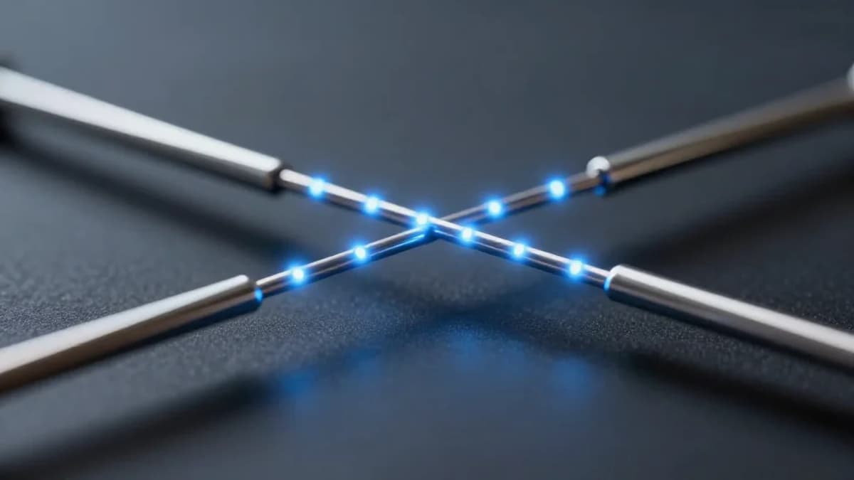
Carbon nanotube (CNT) quantum electronics has long promised atomically precise control, yet material disorder has limited practical adoption. C12’s recent "materials‑first" growth technique produces ultra‑clean, suspended CNTs where intrinsic electronic behavior dominates over defect scattering. This purity is crucial for quantum hardware because it reduces variability in qubit parameters, allowing engineers to design devices with predictable performance rather than compensating for random imperfections. By integrating high‑quality CNTs with advanced semiconductor processing, C12 bridges the gap between laboratory physics and manufacturable quantum components.
The centerpiece of the study is a 15‑gate keyboard architecture that creates a synthetic charge‑density wave along a 4‑micrometer nanotube. By applying alternating voltages, the team induces a controllable Peierls‑like transition, opening an energy gap that can be tuned from 200 µeV up to 30 meV. Crucially, the experiments reveal that a minimum of seven independently modulated gates is needed to establish a clear, stable gap, demonstrating that electrostatic engineering can outweigh residual disorder. This level of gap control directly translates to extended decoherence times, as the insulating state shields qubits from low‑energy excitations that would otherwise cause errors.
Looking ahead, the 15‑gate platform serves as a testbed for engineering Su‑Schrieffer‑Heeger and Kitaev chains, which are theoretical foundations for Majorana modes and other non‑abelian excitations. Such topological constructs could enable qubits that are intrinsically protected from local noise, dramatically simplifying error‑correction overhead. C12’s ability to manipulate the low‑energy spectrum at the nanoscale positions carbon nanotubes as a viable alternative to silicon and superconducting circuits for next‑generation quantum processors, potentially accelerating the race toward scalable, fault‑tolerant quantum computing.
C12 Demonstrates Tunable Metal–Insulator Transition in Ultra-Clean Carbon Nanotubes
0
Comments
Want to join the conversation?
Loading comments...