Caltech Laser Technique Breaches 3,000 K Barrier to Grow Ultra‑Refractory Thin Films
Why It Matters
The ability to deposit ultra‑refractory thin films directly addresses a bottleneck that has limited the performance and scalability of superconducting quantum processors. Current fabrication routes require complex, multi‑step deposition and annealing cycles that introduce defects and increase cost. By simplifying the process, TLE could accelerate the rollout of more reliable qubits, shortening the path to fault‑tolerant quantum computers. Beyond quantum computing, the technique expands the material palette for high‑temperature applications such as hypersonic vehicle coatings, nuclear‑reactor components, and next‑generation power electronics. Industries that have been forced to work around the melting‑point ceiling can now consider designs that exploit the superior mechanical and electrical properties of materials like tantalum and niobium, potentially leading to devices that operate at higher power densities and in harsher environments.
Key Takeaways
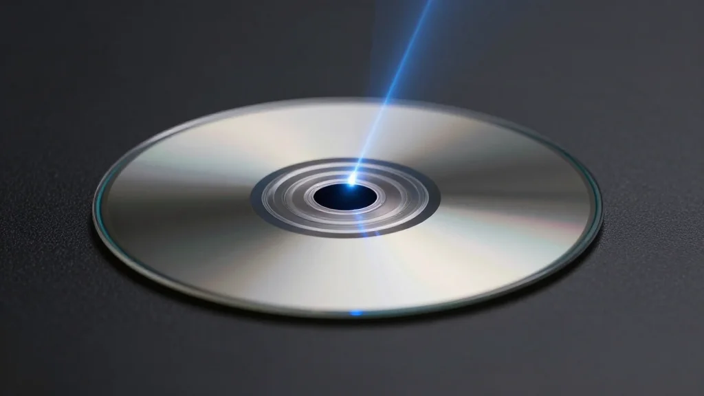
- •Caltech team led by Prof. Austin Minnich used a 1‑kW fiber laser to vaporize ultra‑refractory materials.
- •The laser thermal evaporation (TLE) process surpasses the 3,000 K melting‑point barrier.
- •Nickel films produced by TLE matched or exceeded conductivity of conventional methods.
- •First successful deposition of niobium thin films—critical for superconducting qubits—was demonstrated.
- •Funding came from a Caltech De Logi Science and Technology Grant; commercial scaling is planned.
Pulse Analysis
The laser‑driven deposition breakthrough is more than a laboratory curiosity; it rewrites the economics of ultra‑refractory material manufacturing. Historically, the high‑temperature barrier forced companies to outsource thin‑film production to a few specialized facilities equipped with exotic crucibles and inert‑gas furnaces, inflating costs and limiting design flexibility. TLE sidesteps those constraints by localizing heat to a micron‑scale region, effectively turning the material itself into its own crucible. This paradigm shift mirrors the way additive manufacturing disrupted metal‑part supply chains a decade ago, suggesting a similar democratization could occur for high‑temperature nanomaterials.
From a competitive standpoint, the United States now hosts its first operational laser deposition instrument for ultra‑refractory films, giving domestic quantum‑hardware firms a strategic advantage over overseas rivals that still rely on conventional sputtering. If Caltech can partner with semiconductor foundries to integrate TLE into existing fab lines, the technology could become a differentiator for U.S. companies seeking to scale superconducting qubit production. The timing aligns with the broader push for quantum‑computing leadership, where material quality directly translates to qubit coherence times and error rates.
Looking ahead, the key challenges will be throughput and uniformity across larger substrates. Scaling a 1‑kW laser to wafer‑scale production will require advances in beam shaping and real‑time plume monitoring. Nonetheless, the proof‑of‑concept results—especially the near‑perfect electrical performance of nickel films—provide a solid foundation for engineering solutions. If those hurdles are cleared, TLE could unlock a new class of high‑temperature nanodevices, from aerospace coatings that survive re‑entry heating to next‑generation power electronics that operate at temperatures previously deemed unattainable.
Caltech Laser Technique Breaches 3,000 K Barrier to Grow Ultra‑Refractory Thin Films
Comments
Want to join the conversation?
Loading comments...