Cambridge Researchers Unveil First LED Powered by Insulating Lanthanide Nanoparticles
Why It Matters
The ability to electrically drive lanthanide‑doped nanoparticles opens a new class of optoelectronic devices that combine the unrivaled spectral purity of rare‑earth emitters with the practicality of solid‑state LEDs. This convergence could dramatically lower the cost and complexity of near‑infrared imaging systems, making high‑resolution diagnostics more accessible in clinical settings. Moreover, the narrow emission bandwidth aligns with the needs of high‑capacity optical communication, where channel isolation is paramount. Beyond immediate applications, the molecular‑antenna concept demonstrates a versatile strategy for interfacing insulating nanomaterials with electronic circuits. This could inspire similar approaches for other quantum materials—such as single‑photon emitters or spintronic components—expanding the toolbox for engineers seeking to harness exotic nanoscale properties without sacrificing electrical compatibility.
Key Takeaways
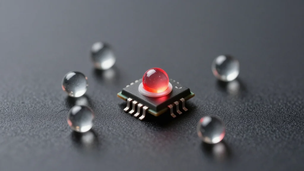
- •Cambridge team creates first LED powered by insulating lanthanide‑doped nanoparticles (LnNPs).
- •Hybrid device uses 9‑anthracenecarboxylic acid as a molecular antenna to achieve >98% triplet‑energy transfer efficiency.
- •LnLEDs operate at ~5 V and emit ultra‑pure light in the second near‑infrared window (≈1000‑1350 nm).
- •Spectral width is narrower than that of quantum‑dot LEDs, offering advantages for imaging and communications.
- •Researchers aim for wafer‑scale production within 12‑18 months, targeting medical imaging, wearable sensors, and secure optical links.
Pulse Analysis
The Cambridge breakthrough redefines the design space for near‑infrared emitters. Historically, the industry has been forced to choose between spectral purity (lanthanide dopants) and electrical drivability (semiconductor quantum dots). By inserting a molecular antenna layer, the researchers have effectively decoupled these constraints, allowing each material to play to its strengths. This could trigger a wave of hybrid architectures where organic and inorganic components are co‑engineered for optimal charge transfer, reminiscent of the early days of organic photovoltaics but now applied to light emission.
From a market perspective, the timing is fortuitous. The global near‑infrared imaging market is projected to exceed $5 billion by 2030, driven by oncology, neurology, and point‑of‑care diagnostics. Current systems rely on expensive laser diodes or bulky fiber‑optic setups. A low‑voltage, chip‑scale LED that delivers comparable or superior performance could compress the value chain, enabling new entrants and accelerating adoption in resource‑limited settings. In parallel, the telecommunications sector is exploring free‑space optical links for data centers and satellite constellations; the narrow linewidth of LnLEDs could support higher channel densities than existing LEDs.
However, commercialization will hinge on overcoming materials‑integration challenges. The organic antenna must survive prolonged electrical stress and environmental exposure, a known weak point for many hybrid devices. Scaling the deposition of 9‑ACA onto nanoparticle films without compromising uniformity will require process innovations, perhaps leveraging atomic‑layer deposition or roll‑to‑roll printing. If these hurdles are cleared, the technology could set a new benchmark for efficiency and spectral control, reshaping both the nanotech and optoelectronics landscapes.
Cambridge Researchers Unveil First LED Powered by Insulating Lanthanide Nanoparticles
Comments
Want to join the conversation?
Loading comments...