Chinese Researchers Achieve Record‑Breaking Ultra‑Deep Nanohole Waveguides with Femtosecond Laser
Why It Matters
The ability to create nanohole waveguides with depth‑to‑diameter ratios above 50,000:1 removes a fundamental bottleneck in nanophotonic integration. Current manufacturing techniques struggle to produce high‑aspect‑ratio features in hard substrates, limiting the miniaturization and performance of on‑chip optical components. By unlocking scalable, high‑precision fabrication in sapphire and potentially other wide‑bandgap crystals, the breakthrough could accelerate the rollout of quantum communication links, ultra‑compact sensors, and high‑bandwidth optical interconnects that are essential for future data‑center and AI workloads. Beyond technical performance, the method offers a cost advantage. Conventional approaches rely on multi‑step lithography and etching sequences that are both time‑consuming and expensive. The single‑pulse, laser‑driven process described by Qiu and Zhong reduces the number of steps and eliminates the need for complex mask alignment, which could lower entry barriers for smaller firms and research labs seeking to prototype advanced photonic devices.
Key Takeaways
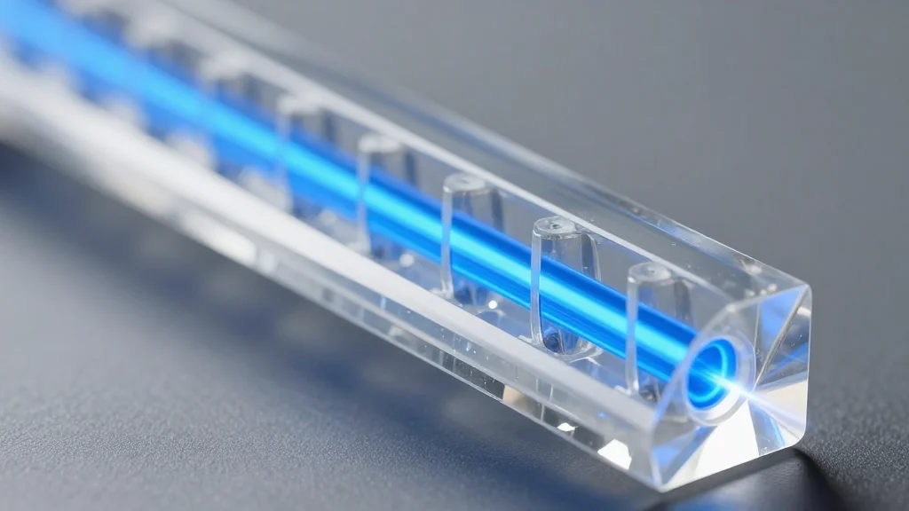
- •Record depth‑to‑diameter ratio >50,000:1 achieved in sapphire nanohole waveguides
- •Sub‑500‑nm diameters and lengths up to 1,500 µm demonstrated
- •Mode purity measured at 10.9 dB with embedded fluorescent probe sensing
- •Technique combines spherical‑aberration‑enhanced focusing, dynamic axial stitching, and wet‑etching‑assisted nanolithography
- •Funding provided by China’s National Natural Science Foundation and Zhejiang Province foundations
Pulse Analysis
The reported ultra‑deep nanohole waveguides represent a paradigm shift in how the industry approaches high‑aspect‑ratio photonic structures. Historically, the trade‑off between depth and feature size forced designers to compromise on either integration density or optical performance. By leveraging spherical‑aberration‑mediated focal stretching, the Chinese team sidestepped the diffraction limit that has constrained femtosecond laser processing for years. This technical insight could be rapidly adopted by research labs worldwide, especially those already equipped with high‑NA femtosecond laser systems.
From a market perspective, the breakthrough aligns with the growing demand for on‑chip quantum photonics. Quantum emitters embedded in hard crystals such as diamond require pristine, low‑loss waveguides to route photons efficiently. The ability to fabricate such waveguides directly in the host crystal eliminates the need for heterogeneous integration, reducing assembly complexity and improving device reliability. Companies developing quantum communication hardware may view this as a strategic advantage, potentially prompting partnerships or licensing deals with the academic teams.
Looking ahead, the key challenge will be translating the laboratory‑scale process into a production‑ready workflow. Issues such as throughput, uniformity across wafer‑scale substrates, and integration with existing CMOS photonic platforms will determine commercial viability. If these hurdles are overcome, the technology could underpin a new generation of ultra‑compact, high‑performance photonic chips that serve everything from data‑center interconnects to biomedical diagnostics, reshaping the competitive landscape of the nanotech sector.
Chinese Researchers Achieve Record‑Breaking Ultra‑Deep Nanohole Waveguides with Femtosecond Laser
Comments
Want to join the conversation?
Loading comments...