Cornell Researchers Use Strain Engineering to Produce Scalable Moiré 2D Materials
Why It Matters
The ability to generate moiré superlattices through strain rather than manual alignment removes a major scalability barrier for quantum‑material research. By fitting within existing semiconductor manufacturing workflows, the technique could accelerate the transition from academic curiosity to market‑ready devices, influencing sectors ranging from quantum computing to ultra‑sensitive detectors. Moreover, the emergence of electrically switchable polarization domains introduces a new functional degree of freedom, potentially enabling novel device architectures that exploit both quantum and classical electronic effects. For the broader nanotech ecosystem, the method demonstrates how conventional process engineering can be repurposed to create exotic material properties. This convergence of mature fabrication tools with frontier physics may inspire similar cross‑disciplinary innovations, fostering a more rapid diffusion of advanced nanomaterials into commercial products.
Key Takeaways
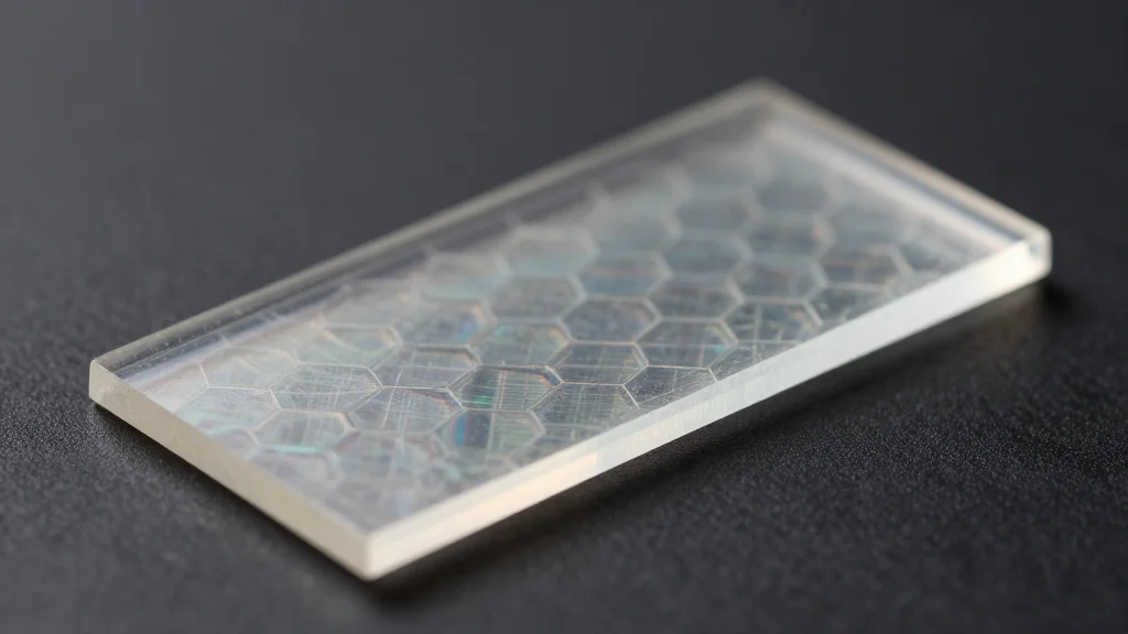
- •Cornell scientists used lithographically patterned stressor films to impose controlled strain on MoS₂, creating moiré patterns without twisting.
- •Both biaxial and uniaxial strain regimes were achieved, producing hexagonal and stripe‑like moiré geometries respectively.
- •The induced strain generated localized electric polarization in normally non‑polar MoS₂, offering a potential switchable nanoscale resistance mechanism.
- •The technique leverages standard thin‑film deposition equipment, aligning with existing semiconductor manufacturing processes.
- •Researchers aim to demonstrate wafer‑scale production and CMOS integration by the end of 2026.
Pulse Analysis
Strain‑based moiré engineering represents a paradigm shift in how the nanotech community approaches quantum‑material synthesis. Historically, the field has been hampered by the manual, low‑throughput nature of twist‑angle control, which limited reproducibility and inflated costs. By co‑opting a well‑established semiconductor process—stress‑induced lattice deformation—Cornell's method effectively democratizes access to moiré physics. This could lead to a surge in experimental activity, as labs without specialized stacking rigs can now fabricate comparable structures using standard cleanroom tools.
From a market perspective, the development lowers the entry barrier for startups seeking to commercialize moiré‑based devices. Venture capital has already shown appetite for quantum‑material platforms, but the lack of a clear manufacturing route has been a risk factor. A scalable, fab‑compatible process mitigates that risk, potentially unlocking new rounds of funding and accelerating the timeline for productization. Companies that can integrate strain‑engineered moiré layers into existing silicon‑based platforms may gain a competitive edge in low‑power electronics and quantum sensing.
Looking ahead, the key challenge will be translating the laboratory‑scale demonstrations into reliable, high‑volume production. Uniformity of strain across large wafers, control of defect densities, and integration with downstream patterning steps will determine whether the approach can move beyond proof‑of‑concept. If these engineering hurdles are overcome, strain‑engineered moiré materials could become a foundational technology for the next generation of quantum devices, much as silicon did for classical computing.
Cornell Researchers Use Strain Engineering to Produce Scalable Moiré 2D Materials
Comments
Want to join the conversation?
Loading comments...