Custom‑Designed Graphene Nanoribbons Achieve Atomic‑Scale Precision for Ultra‑Compact Electronics
Why It Matters
Atomically precise nanoribbons could dramatically shrink the size of electronic components, allowing more functionality per unit area and reducing power consumption. This breakthrough also provides a deterministic design pathway, which is essential for reliable manufacturing of quantum‑grade devices. Beyond transistors, the programmable electronic properties of these ribbons may accelerate the development of nanoscale photonic circuits, flexible wearable sensors, and neuromorphic computing elements, positioning Europe as a leader in next‑generation nanotech manufacturing.
Key Takeaways
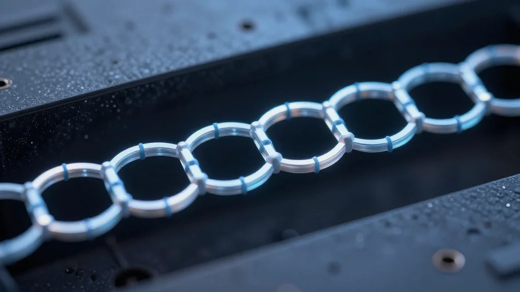
- •Researchers created graphene nanoribbons by directly linking electron donor and acceptor molecules on a gold surface.
- •The method enables atomic‑scale control of electronic properties, eliminating variability of traditional edge‑patterning.
- •Study published in Nature Communications on April 28, 2026, by a team from Birmingham, Warwick and Vienna.
- •Potential applications include sub‑10‑nm transistors, quantum‑dot interconnects and ultra‑dense sensor arrays.
- •Next steps involve scaling the process to wafer‑size substrates and integrating ribbons into prototype devices.
Pulse Analysis
The Birmingham‑Warwick‑Vienna collaboration marks a strategic shift from post‑fabrication tuning to pre‑fabrication design in graphene nanotechnology. Historically, the promise of graphene nanoribbons has been hampered by the inability to reliably control edge geometry and doping, leading to inconsistent electronic behavior. By leveraging donor‑acceptor chemistry—a well‑understood tool in organic electronics—the team sidesteps these bottlenecks, offering a chemically deterministic route that aligns with existing molecular‑scale manufacturing techniques.
From a market perspective, the ability to program bandgaps at the molecular level could revive interest in graphene as a semiconductor alternative, a sector that has seen investment ebb after repeated setbacks. Venture capital has been cautious, favoring silicon‑based scaling, but a clear path to manufacturable, atomically precise components could unlock a new wave of funding. Moreover, the European Union’s emphasis on advanced materials and strategic autonomy may translate into public‑private partnerships that accelerate the transition from laboratory proof‑of‑concept to pilot production.
Looking ahead, the critical challenge will be throughput. On‑surface synthesis under ultra‑high vacuum is inherently slow, and scaling to industrial volumes will demand novel reactor designs or alternative surface chemistries. If the upcoming wafer‑scale pilots succeed, we could see the first generation of molecularly engineered chips within the next five years, potentially redefining Moore’s law’s trajectory and opening a niche for ultra‑low‑power, high‑density devices in edge computing and IoT markets.
Custom‑Designed Graphene Nanoribbons Achieve Atomic‑Scale Precision for Ultra‑Compact Electronics
Comments
Want to join the conversation?
Loading comments...