Defect Engineering in Large‐Scale CVD‐Grown Hexagonal Boron Nitride: Formation, Spectroscopy, and Spin Relaxation Dynamics (Small 8/2026)
•February 6, 2026
0
Companies Mentioned
Why It Matters
Scalable defect engineering in hBN paves the way for mass‑produced quantum photonic components, accelerating commercialization of quantum communication and sensing technologies.
Key Takeaways
- •Optically active hBN defects enable quantum photonics
- •Defect formation controlled by particle energy and substrate
- •Suspended CVD hBN allows precise defect engineering
- •Study maps spectroscopy and spin relaxation dynamics
- •Scalable platform for 2D quantum devices
Pulse Analysis
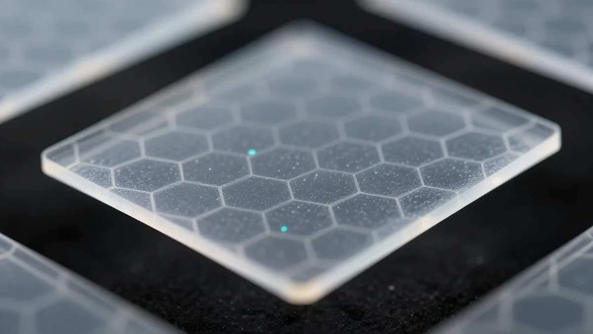
Hexagonal boron nitride has emerged as a leading two‑dimensional host for single‑photon emitters, thanks to its wide bandgap and stable optically active defects. Traditional defect creation relied on localized ion implantation or laser writing, which struggled to maintain uniformity over large areas. The new study leverages chemical vapor deposition to produce continuous hBN films and introduces a suspended‑sample configuration that isolates the material from substrate‑induced strain, enabling uniform defect generation across industrial‑scale wafers.
The authors systematically varied the kinetic energy and species of particles bombarding the hBN lattice, demonstrating that higher energies increase vacancy formation while lighter ions favor substitutional defects. Advanced photoluminescence and electron spin resonance spectroscopy mapped the resulting defect landscape, revealing narrow emission peaks and spin relaxation times suitable for quantum bit operations. Crucially, the spin dynamics were shown to be tunable via the defect’s local environment, offering a controllable platform for quantum information processing without the need for complex cryogenic setups.
From a commercial perspective, this breakthrough addresses two critical bottlenecks: reproducibility and scalability. By integrating defect engineering directly into the CVD workflow, manufacturers can embed quantum emitters during standard wafer fabrication, reducing cost and complexity. The ability to produce centimeter‑scale hBN with consistent quantum properties opens opportunities for on‑chip quantum communication links, high‑resolution magnetic sensing, and hybrid photonic circuits. As the quantum ecosystem matures, such wafer‑compatible defect platforms are likely to become foundational components in next‑generation secure networks and quantum‑enhanced sensors.
Defect Engineering in Large‐Scale CVD‐Grown Hexagonal Boron Nitride: Formation, Spectroscopy, and Spin Relaxation Dynamics (Small 8/2026)
0
Comments
Want to join the conversation?
Loading comments...