Electronic Structure Modulation via Composition‐Preserving Phase Transformations in Metal–Organic Assemblies on the Surface
•February 6, 2026
0
Companies Mentioned
Why It Matters
It provides a practical route to engineer the electronic behavior of surface‑confined metal‑organic networks, expanding design flexibility for catalysis, magnetism and optoelectronic devices.
Key Takeaways
- •Room‑temperature phase change without altering chemical composition
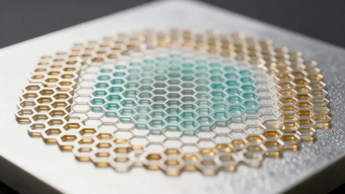
- •Three hexagonal lattices identified via STM/STS
- •Geometric relaxation strengthens Ag–molecule bonds
- •Electronic structure shifts detected by spectroscopy and DFT
- •Enables tunable functionality for surface nanodevices
Pulse Analysis
Metal‑organic coordination assemblies have emerged as a versatile platform for constructing nanoscale functional materials on conductive substrates. Traditionally, altering their electronic properties required changing the molecular precursors, the metal centers, or applying high‑temperature annealing that risks unwanted side reactions. Such approaches often modify the chemical composition, complicating the correlation between structure and function. By contrast, the present study demonstrates that subtle geometric rearrangements—achieved at ambient conditions—can serve as an independent lever for electronic tuning, preserving the original chemical identity of the network.
In the Ag‑carboxylate system derived from 3,5‑dinitrobenzoic acid, scanning tunneling microscopy revealed a stepwise transition among three hexagonal lattices on Ag(111). Each lattice exhibits a distinct packing density and molecular orientation, which DFT calculations link to incremental changes in the Ag‑O bond length and angle. These geometric relaxations enhance orbital overlap between the silver substrate and the coordinated molecules, producing measurable shifts in the local density of states captured by scanning tunneling spectroscopy. The combined experimental‑theoretical workflow underscores how minute structural relaxations can modulate collective electronic bands without introducing new chemical species.
The implications extend beyond academic curiosity. A composition‑preserving, temperature‑friendly method to adjust electronic structure opens new avenues for designing surface‑bound catalysts with optimized charge transfer, magnetic arrays with controllable exchange interactions, and optoelectronic interfaces where band alignment is critical. Future research can explore similar phase‑driven tuning in other metal‑organic frameworks, integrate external stimuli such as electric fields, and scale the approach toward device‑level fabrication. This strategy enriches the toolbox for rational nanomaterial engineering, aligning with industry demands for precise, low‑energy processing techniques.
Electronic Structure Modulation via Composition‐Preserving Phase Transformations in Metal–Organic Assemblies on the Surface
0
Comments
Want to join the conversation?
Loading comments...