Engineering Grain Architecture in Epitaxial Aluminum on Miscut Substrates Toward Various Clean Limits and Giant Superconductivity Modulation
Why It Matters
The ability to tune aluminum’s superconducting properties via substrate miscut offers a scalable pathway to ultraclean quantum‑device platforms, enhancing performance and design flexibility across photonic, electronic, and quantum technologies.
Key Takeaways
- •Miscut angle tunes Al grain size and roughness.
- •Superconducting Tc changes ~10% with grain architecture.
- •Critical current varies up to 100% via miscut control.
- •Magnetic field tolerance increases up to 1000%.
- •Strain drives transition from type‑I to type‑II.
Pulse Analysis
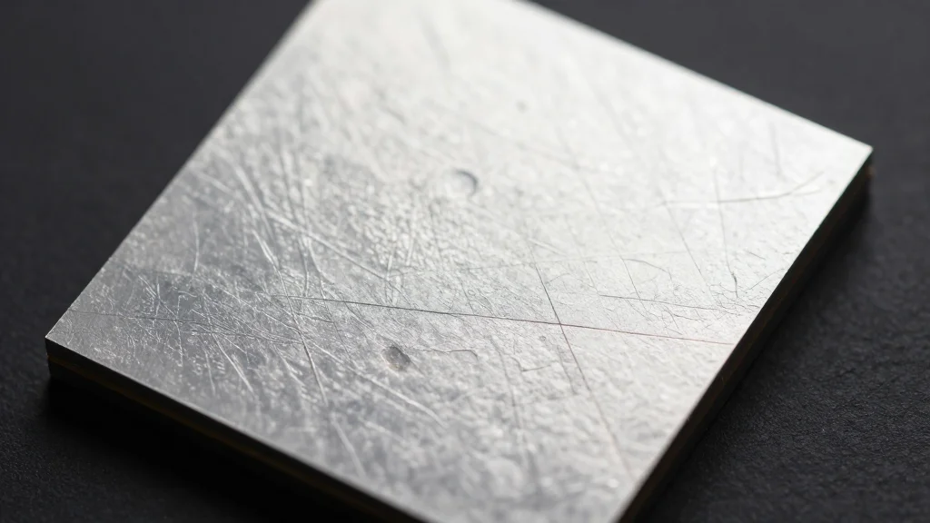
Aluminum’s role in next‑generation photonic and quantum circuits hinges on its crystalline purity. Traditional deposition methods struggle to balance large grain domains with low surface roughness, leading to scattering losses and decoherence. By introducing a controlled miscut on GaAs substrates, researchers can subtly alter the nucleation landscape, fostering either twinned grains or expansive single‑crystal regions. This substrate‑driven approach sidesteps the need for altered temperature or pressure regimes, delivering a versatile toolkit for engineers seeking ultraclean aluminum layers.
The experimental data reveal dramatic superconducting modulation. A modest 10% rise in critical temperature accompanies refined grain structures, while critical current sees a full‑order‑of‑magnitude boost and magnetic‑field resilience spikes by a factor of ten. Crucially, the lattice‑mismatch strain from the miscut not only enhances performance metrics but also reshapes the superconducting phase, prompting a shift from conventional type‑I behavior to a type‑II‑like response. Such a transition expands the operational envelope of Al‑based qubits and detectors, allowing higher magnetic fields without quenching superconductivity.
For industry, this miscut strategy translates into a manufacturable route to tailor superconducting films on a wafer scale. Device designers can now specify substrate tilt angles to meet precise performance targets, reducing reliance on post‑growth processing. The findings also open avenues for integrating aluminum with other lattice‑mismatched materials, potentially unlocking hybrid platforms that combine superconductivity with optoelectronic functionality. Continued exploration of miscut‑induced strain effects promises to refine the balance between crystallinity and mechanical stability, cementing aluminum’s position at the heart of ultra‑low‑noise quantum hardware.
Engineering Grain Architecture in Epitaxial Aluminum on Miscut Substrates Toward Various Clean Limits and Giant Superconductivity Modulation
Comments
Want to join the conversation?
Loading comments...