Engineers Just Created a “Phonon Laser” That Could Shrink Your Next Smartphone
•January 17, 2026
0
Why It Matters
A single‑chip SAW source streamlines RF filtering, cutting device size and power draw while enabling higher‑frequency wireless communication.
Key Takeaways
- •Phonon laser generates SAWs on-chip, eliminating external components
- •Operates at ~1 GHz, surpassing traditional SAW limits
- •Uses silicon, lithium niobate, indium gallium arsenide stack
- •Could shrink smartphones while boosting speed and efficiency
- •Enables single-chip radio processing, simplifying device architecture
Pulse Analysis
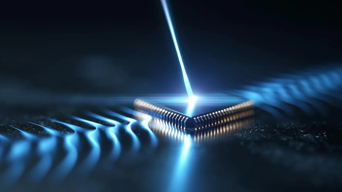
Surface acoustic waves have long been the hidden workhorse behind mobile‑phone filters, GPS receivers and RFID tags, converting radio signals into mechanical vibrations for precise frequency selection. Traditional SAW modules require a pair of chips—one to launch the wave and another to receive it—plus an external bias, which adds bulk and consumes valuable battery power. The new phonon‑laser approach flips this paradigm by creating a self‑sustaining acoustic cavity on a half‑millimeter bar, allowing the wave to bounce, amplify and exit much like light in an optical laser. This compact architecture opens the door to integrating the entire RF front‑end onto a single silicon die.
The breakthrough hinges on a multilayer stack: a silicon substrate for CMOS compatibility, a thin lithium‑niobate film that converts electric fields into surface vibrations, and an indium‑gallium‑arsenide layer that accelerates electrons to feed energy back into the wave. By timing electron injection with the forward‑moving acoustic mode, the device achieves net gain despite a 99% loss on the backward pass. The result is a coherent SAW at roughly 1 gigahertz, with theoretical pathways to tens or even hundreds of gigahertz, dwarfing the frequency ceiling of legacy SAW filters.
For the wireless industry, this could translate into phones that pack more antennas, higher‑bandwidth 5G/6G capabilities, and longer battery life, all within a slimmer chassis. Beyond consumer gadgets, the phonon laser may accelerate advances in radar, quantum sensing and on‑chip signal processing where low‑loss, high‑frequency acoustic control is prized. Scaling the technology will require mastering material interfaces and thermal management, but the proof‑of‑concept published in Nature signals a viable route toward next‑generation acoustic‑photonics integration.
Engineers just created a “phonon laser” that could shrink your next smartphone
0
Comments
Want to join the conversation?
Loading comments...