EPFL Unveils First Integrated Femtosecond Laser on a Chip, Matching Tabletop Performance
Why It Matters
By collapsing a high‑energy femtosecond laser onto a silicon photonic platform, EPFL has removed a fundamental barrier that limited ultrafast optics to large, expensive instruments. The breakthrough could accelerate the diffusion of precision photonics into sectors that demand size, cost and robustness—medical imaging, precision manufacturing, and next‑generation timing. Moreover, the wafer‑scale approach promises economies of scale that could make ultrafast lasers as ubiquitous as LEDs within a decade. The development also reshapes the competitive landscape of integrated photonics. Companies that have focused on telecom‑grade passive waveguides now face a new frontier where active, high‑power light sources can be co‑fabricated. This may spur a wave of investment in silicon‑nitride and other low‑loss platforms, as well as new business models centered on turnkey ultrafast modules for end‑users.
Key Takeaways
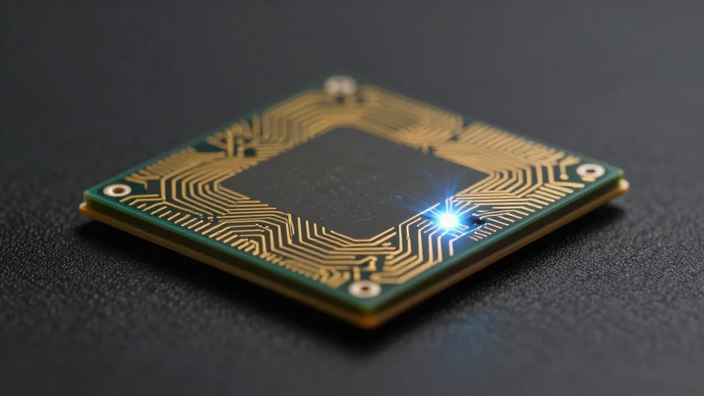
- •EPFL integrated a 1.05 nJ femtosecond laser onto a photonic chip, matching tabletop performance.
- •The chip uses a Mamyshev oscillator architecture to manage dispersion and nonlinearity.
- •Wafer‑scale fabrication could yield >1,000 laser cavities per wafer, reducing costs dramatically.
- •Portable applications include handheld OCT, two‑photon microscopy, and chip‑scale atomic clocks.
- •Next milestones: rugged packaging, wavelength expansion, and commercial pilot programs within 12‑18 months.
Pulse Analysis
The EPFL breakthrough arrives at a moment when the photonics industry is seeking to transition from passive interconnects to active light sources that can be mass‑produced. Historically, ultrafast lasers have been the domain of specialized labs because the delicate balance of dispersion compensation and nonlinear control could not be replicated in micron‑scale waveguides. By demonstrating a viable on‑chip mode‑locked cavity, EPFL not only validates a long‑theorized design but also provides a concrete manufacturing pathway that leverages existing semiconductor fabs.
From a market perspective, the integration lowers the total cost of ownership for ultrafast systems, which have traditionally run into the hundreds of thousands of dollars. If the projected wafer yields hold, the per‑chip price could drop into the low‑thousands, opening new customer segments such as point‑of‑care diagnostics and field‑deployed sensing. This price compression will likely trigger a wave of startup activity focused on application‑specific modules—think portable spectrometers for environmental monitoring or compact frequency combs for next‑generation GPS alternatives.
Strategically, incumbents in the laser industry may need to pivot toward hybrid solutions that combine their expertise in high‑power gain media with EPFL‑style integrated platforms. Partnerships between traditional laser manufacturers and silicon photonics foundries could become the norm, accelerating the convergence of optics and electronics. In the longer term, the ability to embed ultrafast sources directly onto chips could enable entirely new architectures for quantum information processing, where precise timing and high‑peak‑power pulses are essential. EPFL’s achievement thus sets the stage for a cascade of innovations that could redefine how light is generated, manipulated, and applied across the technology stack.
EPFL Unveils First Integrated Femtosecond Laser on a Chip, Matching Tabletop Performance
Comments
Want to join the conversation?
Loading comments...