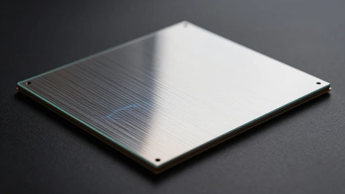
European Consortium Develops Laser Process for Transferring Graphene and Other 2D Materials Onto CMOS-Compatible and Silicon Photonics Wafers
•December 29, 2025
0
Companies Mentioned
Why It Matters
LDT removes a key bottleneck in 2D‑material integration, enabling high‑volume semiconductor and photonics manufacturing and accelerating next‑generation data‑communication devices.
Key Takeaways
- •Laser Digital Transfer enables sub‑10 µm patterning
- •Process works on 4‑inch and 8‑inch wafers
- •No polymers or solvents left after transfer
- •Scalable, automation‑ready for industrial production
- •Opens graphene integration for photonic modulators and sensors
Pulse Analysis
The Laser Digital Transfer (LDT) process marks a paradigm shift for silicon photonics by marrying the unique electronic properties of graphene with the scalability of traditional CMOS fabs. Unlike conventional wet‑transfer methods that rely on polymers and solvents, LDT uses a focused laser pulse to lift and deposit 2D‑material pixels directly onto wafer surfaces. This eliminates contamination risks, preserves material integrity, and aligns with the clean‑room standards required for high‑performance optoelectronic components.
From a manufacturing perspective, LDT’s compatibility with 4‑inch and 8‑inch wafer formats unlocks true wafer‑scale production. The ability to pattern features ranging from sub‑10 µm to half‑millimeter dimensions in a single, digital step reduces cycle time and tool complexity. Automation‑ready workflows mean that foundries can integrate the technology into existing lithography lines, paving the way for cost‑effective mass adoption of graphene‑based modulators, photodetectors, and integrated transceivers that demand ultra‑fast data rates.
Strategically, the European consortium behind L2D2—spanning academia, semiconductor leaders like NVIDIA Mellanox, and specialty material firms—positions Europe at the forefront of next‑generation photonic integration. By solving the long‑standing bottleneck of clean, scalable 2D‑material transfer, the project accelerates the commercialization of high‑speed data‑communication solutions and advanced sensor platforms. This breakthrough could reshape supply chains, drive new revenue streams for chipmakers, and reinforce Europe’s competitive edge in the global semiconductor ecosystem.
European consortium develops laser process for transferring graphene and other 2D materials onto CMOS-compatible and silicon photonics wafers
0
Comments
Want to join the conversation?
Loading comments...