Ga‐Assisted Free‐Standing Growth of CsPbBr3 Nanowires for High‐Performance Optoelectronic Applications
•January 25, 2026
0
Why It Matters
The ability to transfer free‑standing perovskite nanowires expands design flexibility for lasers and photodetectors, accelerating commercialization of high‑efficiency, polarized optoelectronic devices.
Key Takeaways
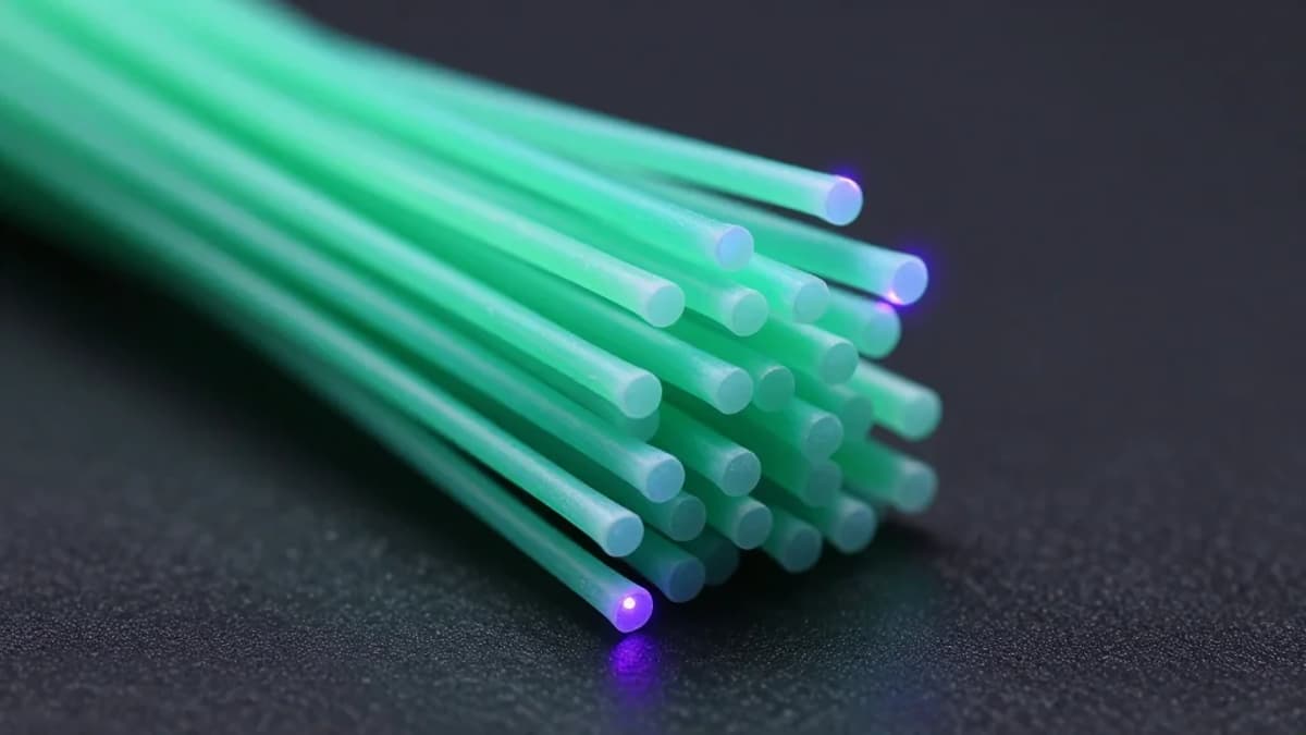
- •Ga‑assisted growth yields free‑standing CsPbBr3 nanowires.
- •Nanowires support single‑mode lasing, polarization ratio 0.908.
- •Photodetector dark current as low as 0.1 pA.
- •Response times under 700 µs, high stability.
- •Transferable to arbitrary substrates for device integration.
Pulse Analysis
The surge of lead‑halide perovskites in photonics stems from their exceptional carrier mobility and tunable bandgaps. Yet, conventional synthesis confines CsPbBr3 nanowires to the substrate surface, limiting post‑growth processing and device architecture flexibility. By introducing gallium as a catalytic assistant, researchers have achieved truly free‑standing nanowires that can be lifted and placed onto any target surface without compromising crystal quality. This breakthrough sidesteps the lithographic constraints that have hampered large‑scale integration of perovskite nanostructures, opening a pathway for modular optoelectronic assembly.
The liberated nanowires act as natural Fabry‑Pérot resonators, delivering single‑mode lasing with a polarization ratio of 0.908—among the highest reported for solution‑processed perovskites. Such strong polarization arises from the intrinsic anisotropy of the one‑dimensional crystal and the high‑Q cavity formed by the wire ends. For applications ranging from on‑chip light sources to polarized displays, this level of control reduces the need for external polarizers, cutting system complexity and power consumption. Moreover, the gallium‑assisted growth is compatible with scalable vapor‑phase techniques, promising cost‑effective manufacturing.
Beyond lasing, the same nanowires power photodetectors that exhibit a dark current of merely 0.1 pA at 1 V and sub‑millisecond rise/fall times, rivaling silicon counterparts while retaining the flexibility of perovskite films. Their environmental resilience—maintaining performance after weeks of ambient exposure—addresses a longstanding reliability hurdle for perovskite devices. As the industry seeks high‑speed, low‑noise sensors for imaging, LiDAR, and wearable electronics, this free‑standing platform offers a versatile, plug‑and‑play solution that could accelerate commercial adoption.
Ga‐Assisted Free‐Standing Growth of CsPbBr3 Nanowires for High‐Performance Optoelectronic Applications
0
Comments
Want to join the conversation?
Loading comments...