Graphene–Perovskite Hybrids Achieve Ultrasensitive Broadband Photodetection
•January 14, 2026
0
Why It Matters
The breakthrough demonstrates a scalable route to ultra‑sensitive, broadband photodetectors suitable for weak‑light imaging and flexible optoelectronics, addressing both performance and stability bottlenecks.
Key Takeaways
- •Inkjet-printed mixed-phase perovskite on graphene.
- •Responsivity reaches 5.7×10⁴ A/W.
- •Detectivity exceeds 10¹⁶ Jones at 312 nm.
- •Phase engineering improves stability and lifespan.
- •Scalable, lithography-free process enables flexible substrates.
Pulse Analysis
Broadband photodetection has long been limited by the trade‑off between sensitivity and material stability. Graphene offers exceptional carrier mobility but lacks intrinsic light absorption, while perovskites provide strong broadband absorption yet suffer from environmental degradation. By marrying these two classes in a hybrid architecture, researchers can exploit graphene’s ultrafast transport to amplify the modest photocurrent generated in the perovskite, creating a powerful photogating effect that dramatically boosts gain without sacrificing speed.
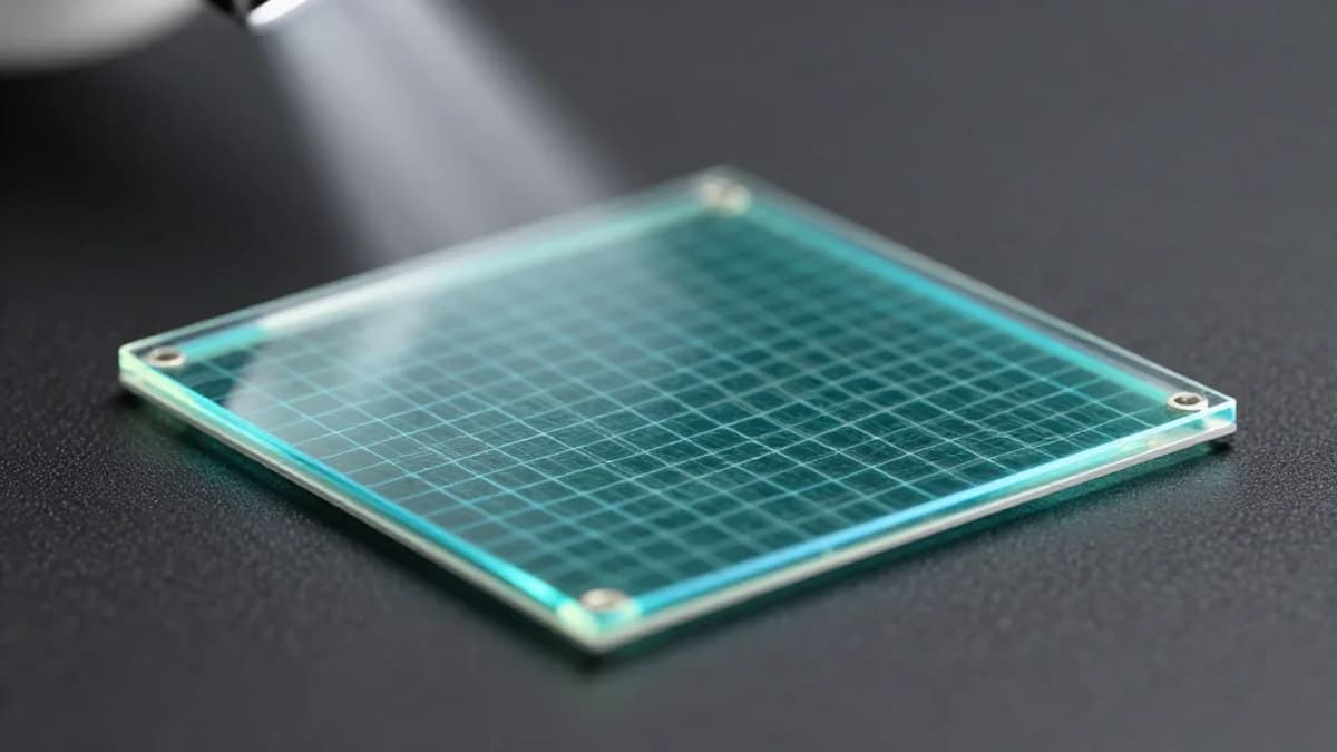
The novel approach leverages maskless inkjet printing to deposit a mixed‑phase CsPbBr₃/Cs₄PbBr₆ film onto a chemical‑vapor‑deposition graphene platform. This “raisin‑bread” morphology creates isolated CsPbBr₃ nanocrystals embedded in a Cs₄PbBr₆ matrix, which both confines charge carriers and shields them from moisture and heat. The resulting devices achieve responsivities above 5.7 × 10⁴ A W⁻¹ and detectivities over 10¹⁶ Jones, rivaling the best reported graphene‑perovskite hybrids while using a lithography‑free, scalable process compatible with roll‑to‑roll manufacturing.
The implications extend beyond laboratory metrics. A fabrication method that avoids photolithography preserves graphene’s pristine lattice, enabling integration onto flexible substrates for wearable imaging, autonomous‑vehicle sensors, and low‑light surveillance systems. Moreover, the demonstrated stability gains address a critical hurdle for commercial perovskite optoelectronics, suggesting a viable pathway toward mass‑produced, high‑performance photodetector arrays. Future work will likely explore further phase engineering, tandem architectures, and large‑scale roll‑to‑roll printing to accelerate adoption in the rapidly growing photonics market.
Graphene–perovskite hybrids achieve ultrasensitive broadband photodetection
0
Comments
Want to join the conversation?
Loading comments...