Illinois Engineers Demonstrate 6× Chip Density Boost with New 3D Stacking Method
Why It Matters
The ability to stack silicon circuits while staying within the 400 °C thermal budget removes a long‑standing barrier to monolithic 3D integration. By delivering six‑fold density gains without new lithography, the method could extend Moore’s law, lower power consumption, and enable more compact, faster memory and logic blocks. This breakthrough also democratizes advanced chip stacking, as it uses standard single‑crystalline silicon and existing fab equipment, potentially accelerating adoption across the semiconductor ecosystem. Beyond the technical merits, the development reshapes competitive dynamics. Companies that can quickly integrate vertical stacking into their product lines may capture market share in high‑performance computing, AI inference, and mobile devices, while laggards risk obsolescence as density and efficiency become decisive factors.
Key Takeaways
- •Illinois Grainger researchers achieved a 6× transistor density increase via vertical stacking.
- •Process respects the 400 °C thermal budget, a key industry constraint.
- •Device yields reported at 98‑100% in academic lab settings.
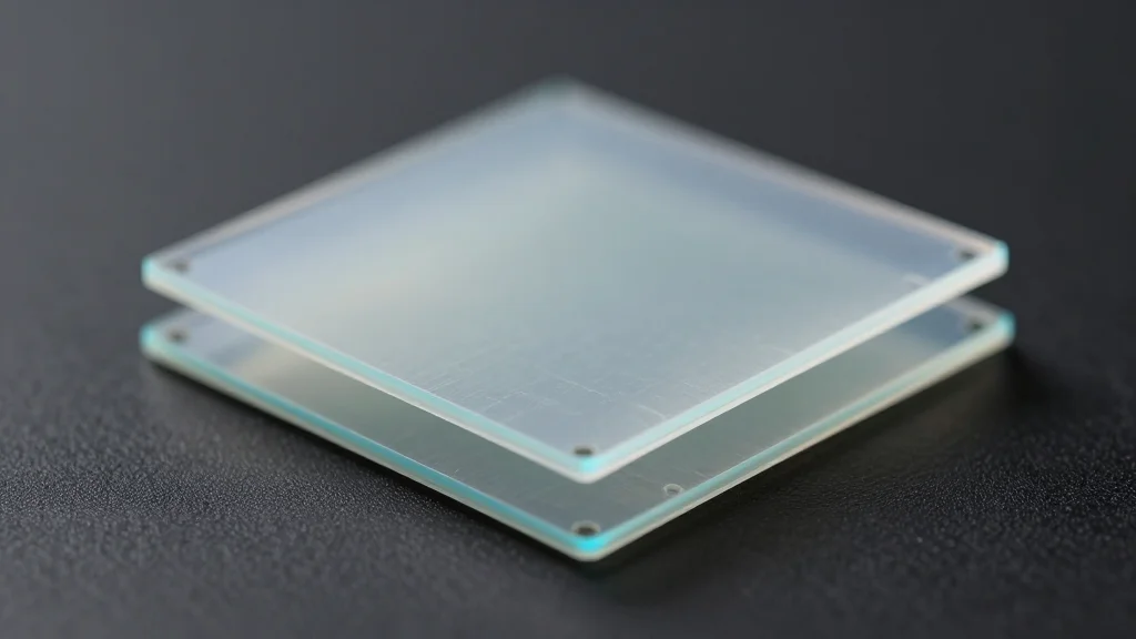
- •Technique uses standard single‑crystalline silicon and roll‑laminator alignment.
- •Potential to extend Moore’s law and reduce power consumption for SRAM and CPUs.
Pulse Analysis
The Illinois team's achievement arrives at a moment when the semiconductor industry is scrambling for alternatives to traditional scaling. While extreme ultraviolet (EUV) lithography has pushed transistor dimensions to the 3‑nm node, the cost and complexity of each new generation are soaring. Vertical integration offers a parallel path: instead of making transistors smaller, make chips taller. The key to commercial viability has always been thermal management; exceeding 400 °C destroys metal interconnects, forcing most 3D approaches to rely on heterogeneous bonding or exotic materials. By proving a monolithic process that stays within this budget, the Illinois team sidesteps the need for costly bonding steps and exotic substrates.
From a market perspective, the breakthrough could catalyze a shift in foundry roadmaps. Major players like TSMC and Samsung have already invested in 3D stacking for specialized AI accelerators, but those solutions are limited to a few layers and require custom packaging. A scalable, wafer‑level stacking method could democratize the technology, allowing a broader set of fabless companies to design 3D‑enabled chips without massive upfront capital. This could compress the performance gap between high‑end data‑center GPUs and more modest edge processors, fueling new AI workloads at the edge.
Looking ahead, the biggest question is speed to volume. The academic results are promising, but translating 98‑100% yields to a 300‑mm fab environment will test process uniformity, defect control, and supply chain readiness. If industry partners can run pilot lines within the next 12‑18 months, we may see the first commercial SRAM products leveraging this stacking method by 2028, setting a new benchmark for density and energy efficiency in the nanotech arena.
Illinois Engineers Demonstrate 6× Chip Density Boost with New 3D Stacking Method
Comments
Want to join the conversation?
Loading comments...