Imaging Ellipsometry Tracks MXene Thin-Film Quality During Fabrication without Damage
Companies Mentioned
Why It Matters
It gives manufacturers a fast, contact‑free way to ensure uniformity and performance of MXene‑based components, accelerating adoption in photodetectors, flexible electronics, and other emerging applications.
Key Takeaways
- •Imaging ellipsometry maps MXene film thickness and conductivity at 1 µm resolution.
- •Two approaches combine spot‑level speed with full‑device spatial coverage.
- •Non‑destructive monitoring tracks property changes during photoresist development.
- •Technique applicable to other 2‑D materials, boosting thin‑film process control.
Pulse Analysis
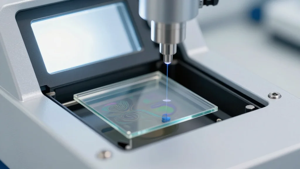
MXenes have emerged as a versatile class of two‑dimensional conductors, promising breakthroughs in photodetectors, energy storage and flexible circuitry. Yet their ultra‑thin nature makes conventional metrology—often invasive or low‑resolution—unsuitable for the tight tolerances required in high‑volume manufacturing. The lack of a reliable, non‑destructive inspection tool has slowed the transition from laboratory prototypes to commercial lines, as manufacturers struggle to detect sub‑nanometer thickness variations and localized conductivity drops that can cripple device yield.
Imaging ellipsometry bridges that gap by exploiting the polarization change of reflected light to extract quantitative film parameters across a wide field of view. The study leverages spectroscopic micro‑ellipsometry (SME) for rapid, high‑precision point measurements and imaging spectroscopic ellipsometry (ISE) for full‑device mapping with lateral resolution down to 1 µm. This dual‑mode workflow delivers real‑time feedback on thickness, composition and charge‑transport properties without contacting the sample, allowing engineers to monitor each lithographic step—especially photoresist development—where traditional probes would risk damage or contamination. The ability to correlate optical signatures with functional performance offers a powerful diagnostic for process optimization.
The broader impact extends beyond MXenes. Because ellipsometry is material‑agnostic, the same platform can be deployed for graphene, transition‑metal dichalcogenides and other emerging 2‑D systems, standardizing thin‑film quality control across the semiconductor supply chain. Early interest from international labs and the open invitation for collaborations suggest rapid uptake in both academic and industrial settings. As manufacturers aim for higher yields and tighter specifications, imaging ellipsometry is poised to become a cornerstone of next‑generation thin‑film fabrication workflows.
Imaging ellipsometry tracks MXene thin-film quality during fabrication without damage
Comments
Want to join the conversation?
Loading comments...