Increased Series Resistance in the Laser‐Enhanced Contacts of Polysilicon‐Based Solar Cells From an Additional Light Anneal
•January 22, 2026
0
Why It Matters
Series‑resistance growth directly erodes power conversion efficiency, making process sequencing critical for next‑generation silicon photovoltaics.
Key Takeaways
- •Light anneal after laser contact raises series resistance
- •Hydrogen accumulates at metal/p+ interface
- •Increased resistance reduces cell efficiency
- •Laser-enhanced contact should be final fabrication step
- •No thick glass layer detected by microscopy
Pulse Analysis
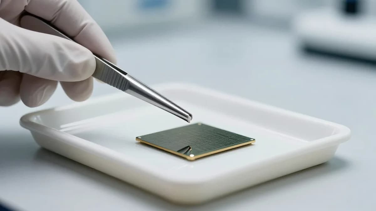
TOPCon (tunneling oxide passivating contact) cells have become a cornerstone of high‑efficiency silicon photovoltaics, leveraging a thin oxide layer and doped polysilicon to achieve low recombination and high open‑circuit voltage. A conventional light‑anneal, performed at moderate temperature under controlled illumination, diffuses hydrogen into the wafer, passivating bulk and surface defects. This step traditionally follows the firing of metallization and has been credited with boosting voltage and overall cell performance across the industry.
The new study reveals a paradox when light‑annealing follows a laser‑enhanced contact process. While hydrogen passivation remains beneficial, excessive hydrogen migrates to the metal/p+ emitter junction, forming a conductive barrier that elevates series resistance. Luminescence imaging highlighted dark regions corresponding to higher resistance, and temperature‑dependent electrical measurements pointed to hydrogen‑induced interface degradation rather than a physical glass layer. The result is a measurable drop in fill factor and power output, underscoring that timing of each thermal step is as crucial as its temperature.
For manufacturers, the implication is clear: the laser‑enhanced contact should be the terminal step in the TOPCon workflow. By eliminating a post‑laser light‑anneal, producers can retain the low‑resistance benefits of laser processing while still capturing hydrogen‑related passivation earlier in the line. This insight guides equipment scheduling, cost modeling, and quality‑control protocols, ensuring that the push toward >25% efficient silicon modules remains on track. Future research may explore alternative hydrogen‑management strategies or in‑situ diagnostics to fine‑tune interface chemistry without sacrificing the gains of laser‑enhanced contacts.
Increased Series Resistance in the Laser‐Enhanced Contacts of Polysilicon‐Based Solar Cells from an Additional Light Anneal
0
Comments
Want to join the conversation?
Loading comments...