Intermediate Phases Unlock Faster Nanoparticle Crystallization
•March 3, 2026
0
Why It Matters
Accelerated, defect‑free nanocrystal production cuts costs and boosts performance for data‑storage, optics, and other high‑tech applications, reshaping material engineering strategies.
Key Takeaways
- •Mesophases lower crystallization free‑energy barriers
- •Simulations show up to orders‑of‑magnitude speed increase
- •Intermediate phases improve crystal quality by reducing defects
- •Design rules enable controlled nanoparticle assembly
- •Approach applicable to polymers and protein self‑assembly
Pulse Analysis
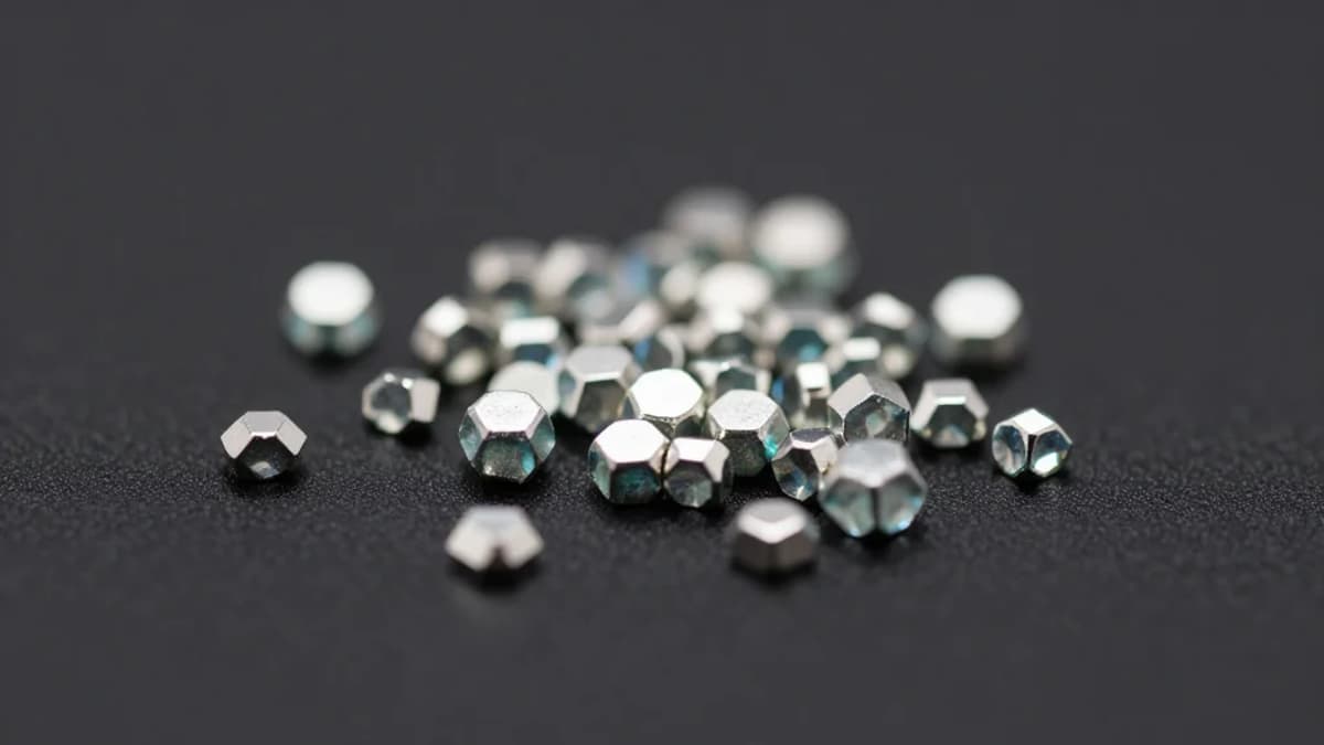
Crystalline nanomaterials underpin next‑generation data‑storage chips, photonic components, and quantum devices, yet steering nanoparticles into a perfect lattice remains a bottleneck. Traditional routes force particles to overcome a single, steep free‑energy barrier, often trapping them in metastable disorder. The Cornell team highlights mesophases—intermediate states such as liquid‑crystalline nematics—as natural waypoints that soften this barrier. By occupying a partially ordered regime, particles gain mobility while aligning orientation, creating a “golden path” toward the final crystal. This insight reframes self‑assembly from a binary jump to a staged progression.
Using high‑resolution molecular dynamics, Fernando Escobedo and B.P. Prakash mapped the transition pathways of several nanoparticle chemistries. Across all models, trajectories that passed through a mesophase crystallized up to ten times faster, and in some systems the rate acceleration reached two orders of magnitude. The simulations also quantified a reduction in the activation free energy, effectively splitting a one‑meter jump into two half‑meter steps. Moreover, the intermediate phase acted as a defect‑annealing environment, yielding crystals with markedly lower dislocation densities. These quantitative design rules give engineers a predictive toolkit for tuning temperature, concentration, and particle shape to invoke the desired mesophase.
The ramifications extend beyond inorganic nanocrystals. Polymers, protein aggregates, and even metal‑organic frameworks often traverse comparable intermediate states, suggesting that intentional mesophase engineering could streamline a broad swath of material synthesis. For industry, faster, higher‑purity nanocrystals translate into lower production costs, tighter tolerances, and accelerated time‑to‑market for devices ranging from magnetic memory to optical sensors. Future work will likely explore experimental validation, scalable processing methods, and integration with additive manufacturing. As the field embraces these stepping‑stone strategies, the balance of speed, quality, and energy efficiency in nanomaterial fabrication is poised for a fundamental shift.
Intermediate phases unlock faster nanoparticle crystallization
0
Comments
Want to join the conversation?
Loading comments...