Ion‐Induced Hydrophilic Switching Enables Nanostructure Morphology Control for Superior Nanoplasmonic Sensing
•January 22, 2026
0
Why It Matters
Uniform nanostructures enable more reliable, high‑sensitivity plasmonic sensors, accelerating wafer‑scale production of next‑generation photonic technologies.
Key Takeaways
- •SF6 plasma makes glass surface hydrophilic.
- •Hydrophilic surface boosts Au adatom mobility during dewetting.
- •Uniform nanoislands reduce size dispersion and gap variance.
- •Refractive-index sensitivity improves 17.8% to 95.21 nm/RIU.
- •Phase‑field model predicts morphology via adhesion term α.
Pulse Analysis
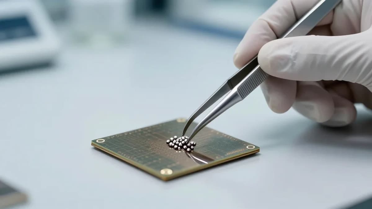
The breakthrough hinges on ion‑induced hydrophilic switching, a surface‑chemistry trick that transforms ordinary glass into a high‑energy platform for gold atoms. By exposing the substrate to a short SF6 plasma burst, surface fluorine species create polar groups that attract water molecules, effectively lowering the contact angle. This altered interfacial energy accelerates Au adatom diffusion during the subsequent thermal dewetting step, allowing the metal film to break up into evenly spaced nanoislands without the need for costly lithographic patterning.
Uniform nanoisland arrays directly translate into superior LSPR sensor characteristics. Smaller size variance and consistently narrow gaps sharpen the plasmonic resonance, increasing the shift per refractive‑index unit and delivering a 17.8% sensitivity gain compared with untreated substrates. The tighter spectral response also improves signal‑to‑noise ratios, making the sensors more reliable for real‑world biochemical detection where reproducibility across wafers is critical. These performance lifts are achieved while maintaining a simple, wafer‑compatible process that can be scaled to industrial volumes.
Beyond the experimental results, the authors integrate a modified Cahn–Hilliard phase‑field model that embeds an explicit adhesion parameter (α) to capture the substrate‑metal interaction. This theoretical framework not only mirrors the observed morphology but also serves as a predictive tool for tailoring film thickness, annealing temperature, and plasma exposure to target specific nanostructure dimensions. By coupling surface‑wetting engineering with physics‑based simulation, the work establishes a roadmap for designing next‑generation plasmonic and photonic devices that balance performance, manufacturability, and cost.
Ion‐Induced Hydrophilic Switching Enables Nanostructure Morphology Control for Superior Nanoplasmonic Sensing
0
Comments
Want to join the conversation?
Loading comments...