Israeli‑Japanese Team Unveils Near‑Zero‑Power Graphene Switch for Brain‑Like Electronics
Why It Matters
The graphene switch represents a paradigm shift in how electronic state changes can be achieved, moving from charge‑based switching to mechanical layer sliding. This approach could dramatically lower the power envelope of future processors, addressing one of the most pressing constraints in scaling AI and edge computing. Moreover, the ability to create inter‑island communication mimics synaptic behavior, offering a hardware foundation for neuromorphic architectures that could outperform conventional chips in pattern‑recognition and adaptive tasks. Beyond computing, the technology could enable a new class of autonomous nanodevices that operate for years on a single charge, expanding possibilities in environmental monitoring, personalized medicine, and smart wearables. By demonstrating that atomic‑scale motion can be harnessed with negligible energy, the work opens avenues for other two‑dimensional materials to be engineered for similarly efficient functions, potentially catalyzing a wave of low‑power nanotechnologies across multiple sectors.
Key Takeaways
- •Israeli‑Japanese team creates graphene switch that requires virtually no power, published in Nature Nanotechnology.
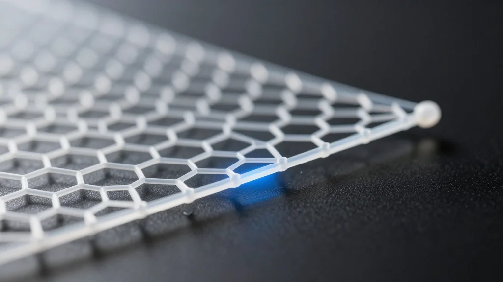
- •Switch built from tens‑of‑nanometers graphene islands that slide layers to change stacking without breaking bonds.
- •Mechanical communication between islands mimics neuronal signaling, enabling neuromorphic computing concepts.
- •Potential to cut energy use of transistors by orders of magnitude, reducing heat and extending battery life for IoT devices.
- •Next steps include scaling the design for commercial circuits and partnering with semiconductor manufacturers.
Pulse Analysis
The near‑zero‑power graphene switch arrives at a moment when the semiconductor industry is grappling with the end of Moore's Law and the soaring energy demands of AI workloads. Traditional scaling has hit physical limits, prompting a search for fundamentally new switching mechanisms. By leveraging frictionless sliding of atomic layers, the Israeli‑Japanese team sidesteps the thermodynamic ceiling that constrains charge‑based transistors, offering a route to continue performance gains without proportional power penalties.
Historically, graphene has been touted for its exceptional conductivity and strength, yet practical applications have been hampered by difficulties in controlling its electronic properties. This breakthrough demonstrates that precise nanoscale patterning can unlock functional behavior previously deemed theoretical. If the community can translate the laboratory‑scale islands into manufacturable patterns, the technology could become a cornerstone for neuromorphic chips that process information in parallel, akin to the brain, and do so with a fraction of the energy budget of current GPUs.
Looking ahead, the commercial viability will hinge on integration with existing fab lines and the ability to produce uniform islands at wafer scale. Partnerships with established semiconductor firms could accelerate this transition, but the path is fraught with material‑science challenges, such as maintaining layer alignment and preventing contamination. Nonetheless, the announcement injects fresh optimism into the nanotech sector, suggesting that atomically engineered devices may finally deliver on the promise of ultra‑low‑power, brain‑inspired computing.
Israeli‑Japanese Team Unveils Near‑Zero‑Power Graphene Switch for Brain‑Like Electronics
Comments
Want to join the conversation?
Loading comments...