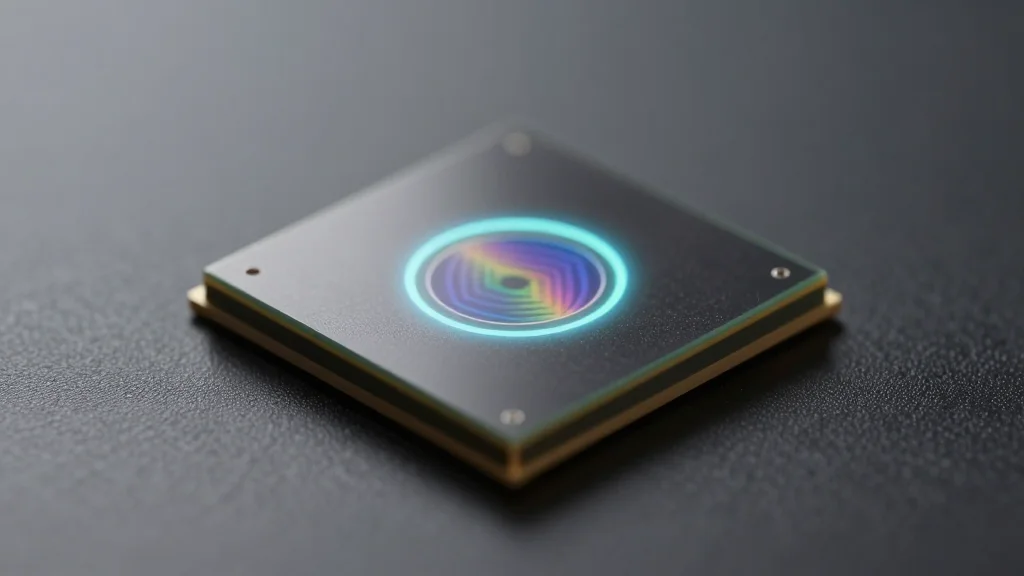
KAIST Microcomb Chip Generates 22 GHz Low‑Noise Signals for Future 6G Networks
Why It Matters
The KAIST microcomb chip showcases how nanofabricated photonic devices can overcome the physical limits of electronic oscillators, a critical hurdle for the rollout of 6G networks that require unprecedented bandwidth and signal fidelity. By proving that sub‑femtosecond timing stability is achievable on a chip‑scale platform, the work signals a shift toward optical‑RF convergence, which could reshape the supply chain for high‑frequency components across telecommunications, automotive safety and space instrumentation. Beyond immediate applications, the research underscores the broader potential of nanotech‑enabled photonics to deliver low‑power, highly integrated solutions for data‑intensive systems. As the industry pushes toward terahertz communications and quantum‑grade timing, the microcomb architecture may become a foundational building block, driving new business models and spurring collaborations between universities, semiconductor foundries and network operators.
Key Takeaways
- •KAIST team led by Prof. Kim Jungwon and Prof. Lee Han‑Suk generated 22 GHz ultra‑low‑noise signals on a microcomb chip.
- •Timing error measured at just 3 femtoseconds, with negligible noise up to 66 GHz.
- •Microcomb uses a "perfect soliton crystal" to lock optical pulses, enhancing stability and reducing power consumption.
- •Potential applications span 6G mobile networks, autonomous‑driving radar, and high‑resolution space observation.
- •Researchers aim to extend operation beyond 300 GHz and begin field trials with a Korean telecom operator later this year.
Pulse Analysis
The microcomb breakthrough arrives at a pivotal moment when the telecom industry is scrambling to define the architecture of 6G. Traditional silicon‑based RF front‑ends are hitting thermal and noise ceilings as carrier frequencies climb into the millimeter‑wave and sub‑terahertz domains. By moving the frequency generation into the optical domain, KAIST sidesteps those constraints, offering a path to both higher frequencies and tighter phase noise specifications. This could force a re‑evaluation of the current RF‑centric roadmaps of major chipmakers like Qualcomm and MediaTek, who may need to incorporate photonic foundry services into their design flows.
From a competitive standpoint, the microcomb’s sub‑femtosecond stability rivals the performance of bulkier optical clock systems that have been confined to laboratory settings. If KAIST can translate this lab‑scale performance into a manufacturable product, it would give South Korean photonics firms—such as Hanwha Systems and LG Innotek—a strategic advantage in the global 6G supply chain. Moreover, the low‑power nature of the chip aligns with the energy‑efficiency targets of autonomous‑vehicle manufacturers, potentially opening a new revenue stream for automotive suppliers.
Looking ahead, the key challenge will be integration. Marrying the microcomb with CMOS drivers and ensuring reliability across automotive temperature ranges will require substantial engineering effort and capital investment. However, the promise of a unified photonic‑RF platform that can serve both communications and sensing markets could justify the expense, especially as governments worldwide earmark billions of dollars for 6G research. In short, KAIST’s microcomb not only solves a technical problem—it reshapes the economic calculus for the next generation of high‑frequency technologies.
KAIST Microcomb Chip Generates 22 GHz Low‑Noise Signals for Future 6G Networks
Comments
Want to join the conversation?
Loading comments...