Laser-Modified Graphene Enables Molecule-Thick Films to Grow only Where Needed
Why It Matters
Selective deposition reduces material waste and unlocks new design freedom for semiconductor and optoelectronic components, accelerating commercialization of next‑generation devices.
Key Takeaways
- •Laser-modified graphene directs molecular layer deposition to selected areas
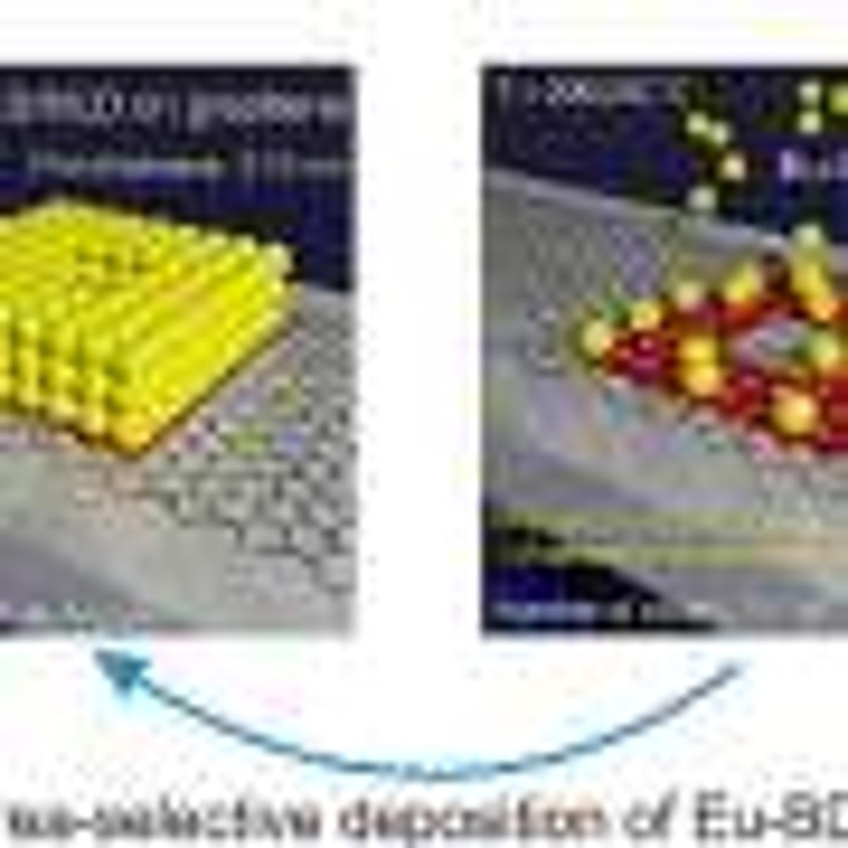
- •One‑molecule‑thick europium‑organic films grow only on functionalized spots
- •Area‑selective ALD enables custom-shaped thin‑film patterns
- •Method combines graphene laser functionalization with molecular layer deposition
- •Potential applications include photoluminescent devices and advanced electronics
Pulse Analysis
Atomic layer deposition (ALD) has long been the workhorse for creating uniform, atom‑by‑atom films in semiconductor manufacturing. Yet conventional ALD coats every exposed surface, limiting designers who need patterned layers for complex architectures. The new laser‑modified graphene method flips this paradigm by turning graphene into a programmable substrate: a focused laser creates hydroxyl‑rich zones that act as chemical anchors, while untouched graphene remains inert. This selective reactivity means that subsequent molecular layer deposition (MLD) deposits material only where the laser has written, delivering true area‑selective growth without additional masking steps.
In the proof‑of‑concept experiment, the team deposited a europium‑organic compound that emits visible light, forming a monolayer exclusively on the laser‑treated patches. Because the film thickness is controlled at the molecular level, manufacturers can engineer optical properties with unprecedented precision, tailoring emission wavelength, intensity, and pattern geometry simultaneously. The technique is compatible with existing silicon wafer processes and can be extended to other two‑dimensional materials, opening pathways for integrated photonic circuits, quantum‑dot arrays, and ultra‑thin sensor coatings.
The commercial implications are significant. By eliminating blanket coating and subsequent etching, the process cuts material waste, reduces cycle time, and lowers production costs for high‑value components such as micro‑LED displays, flexible electronics, and next‑generation memory. Moreover, the ability to embed functional organometallic layers in defined regions could accelerate the rollout of on‑chip light sources and bio‑compatible interfaces. Companies interested in advanced nanofabrication are encouraged to collaborate with the research team to translate this laboratory breakthrough into scalable manufacturing solutions.
Laser-modified graphene enables molecule-thick films to grow only where needed
Comments
Want to join the conversation?
Loading comments...