Low‐Voltage, High‐Sensitivity NIR Ambipolar Organic Phototransistor Based on a Non‐Fullerene Acceptor
•March 3, 2026
0
Why It Matters
The breakthrough enables energy‑efficient, flexible NIR imaging and detection, accelerating adoption of organic optoelectronics in wearables, IoT, and biomedical monitoring.
Key Takeaways
- •Y6 provides strong NIR absorption and ambipolar transport
- •ODPA SAM improves Al2O3 dielectric interface, reducing traps
- •Device operates below 5 V, enabling low‑power applications
- •Responsivity and detectivity surpass previous organic NIR phototransistors
- •Fast response (tens‑hundreds ms) suitable for real‑time imaging
Pulse Analysis
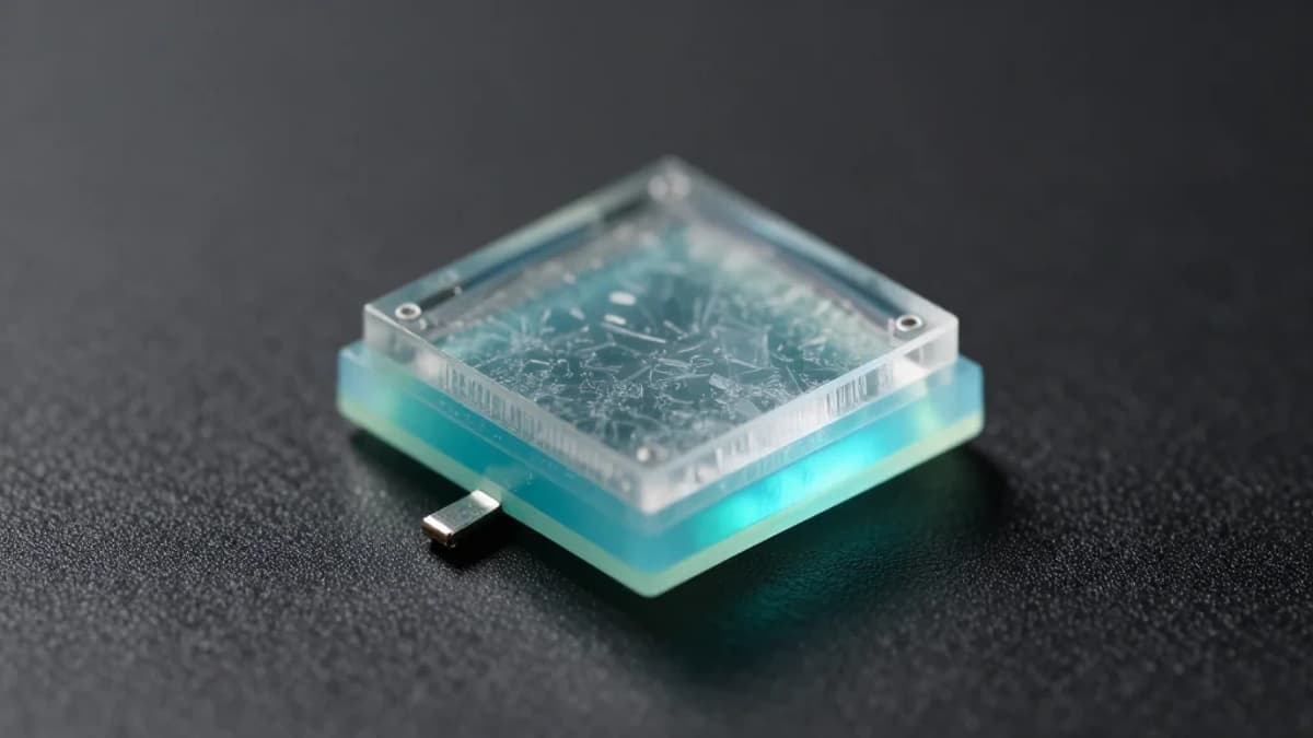
The emergence of non‑fullerene acceptors like Y6 is reshaping organic optoelectronics, especially for near‑infrared applications where traditional fullerene systems fall short. Y6’s broad NIR absorption combined with balanced electron‑hole mobility enables ambipolar operation, a rare feat that simplifies circuit design and reduces component count. By pairing Y6 with a high‑k Al2O3 dielectric and fine‑tuning the interface through an octadecylphosphonic acid (ODPA) self‑assembled monolayer, researchers have mitigated trap states that typically limit organic phototransistor speed and sensitivity.
Low‑voltage operation is a critical metric for emerging wearable and Internet‑of‑Things (IoT) devices that rely on battery or energy‑harvesting power sources. The demonstrated ≤5 V bias not only cuts power consumption but also eases integration with standard flexible substrates and printed electronics processes. High responsivity and detectivity, coupled with response times in the sub‑second regime, position this Y6‑based phototransistor as a viable alternative to inorganic NIR detectors, which often require complex fabrication and cooling.
Looking ahead, the platform’s scalability and compatibility with roll‑to‑roll manufacturing could drive cost‑effective production of flexible NIR imaging arrays, smart textiles, and point‑of‑care diagnostic sensors. As the industry pushes for greener, lightweight, and low‑power photonic components, the combination of non‑fullerene acceptors and interface‑engineered dielectrics is likely to become a cornerstone of next‑generation organic optoelectronic systems.
Low‐Voltage, High‐Sensitivity NIR Ambipolar Organic Phototransistor Based on a Non‐Fullerene Acceptor
0
Comments
Want to join the conversation?
Loading comments...