Maskless Laser Printing Enables 3D Carbon Circuits on Glass, Paving Way for Next‑Gen Chip Packaging
Why It Matters
The ability to print 3‑D carbon circuits on glass without masks directly addresses a critical cost and complexity barrier in advanced semiconductor packaging. As AI workloads push for denser, faster chip stacks, manufacturers need interconnect solutions that combine high thermal performance with fine‑pitch routing. Mask‑less laser printing could slash production steps, lower defect rates, and enable new form factors such as 3‑D stacked sensors and quantum devices. Moreover, extending the process to metals would further disrupt traditional metallization techniques, potentially reshaping the supply chain for high‑performance packaging. Beyond cost, the technology offers design flexibility. Engineers can rapidly prototype interconnect layouts on curved or through‑hole glass structures, accelerating innovation cycles for emerging applications like photonic‑electronic integration and on‑chip optics. If the promised scalability materializes, the method could become a cornerstone of next‑generation packaging standards, influencing everything from data‑center processors to edge AI chips.
Key Takeaways
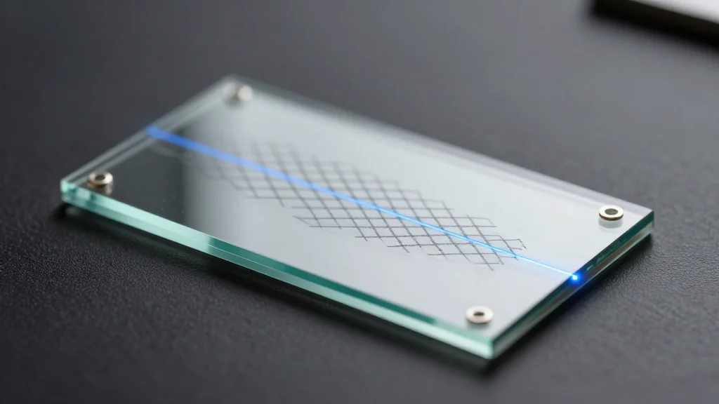
- •Mask‑less ULCVD uses a 1040 nm femtosecond laser to directly write carbon circuits on glass
- •All‑surface capability enables patterning on front, rear, through‑holes and curved geometries
- •Carbon lines achieve conductivity comparable to top‑performing laser‑induced graphene
- •Technique eliminates multi‑step masking, reducing cost and cycle time
- •Researchers aim to extend the process to copper and gold for full‑metal interconnects
Pulse Analysis
The ULCVD breakthrough arrives at a pivotal moment when the semiconductor industry is grappling with the "packaging wall"—the point at which interconnect limitations throttle system‑level performance. Traditional photolithography, while mature, is increasingly ill‑suited for the three‑dimensional routing required by heterogeneous integration. By leveraging femtosecond‑laser physics, the Korean‑American consortium sidesteps the diffraction limits and thermal damage that have hampered prior laser‑based approaches, delivering clean, graphitic pathways that meet the conductivity demands of high‑frequency signaling.
From a market perspective, the technology could erode the value proposition of established mask‑making suppliers and lithography equipment vendors, especially in the niche of advanced packaging where volumes are lower but margins are high. Companies like ASML and TEL have invested heavily in EUV and DUV lithography for front‑end processes; a mask‑free back‑end solution could diversify the equipment landscape and open new revenue streams for laser manufacturers such as Coherent and IPG Photonics. However, the path to volume production will hinge on demonstrating repeatable metal deposition, as the industry still relies on copper and gold for low‑resistance interconnects.
Looking ahead, the research team’s roadmap—moving from carbon to metal—mirrors the broader industry trend toward monolithic integration of diverse materials. If successful, ULCVD could become the linchpin for next‑gen chiplets that combine logic, memory, photonics, and quantum sensors on a single glass platform. The key challenges will be scaling laser throughput to wafer‑level speeds, ensuring uniformity across large substrates, and integrating the process into existing fab lines without compromising yield. Stakeholders should watch for pilot production announcements in the coming months, as they will signal whether this academic breakthrough can translate into a commercial standard that reshapes the economics of advanced semiconductor packaging.
Maskless Laser Printing Enables 3D Carbon Circuits on Glass, Paving Way for Next‑Gen Chip Packaging
Comments
Want to join the conversation?
Loading comments...