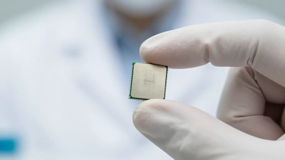
Miniaturized Self‐Powered Perovskite Spectrometer
•January 25, 2026
0
Companies Mentioned
Why It Matters
The breakthrough enables affordable, low‑power spectroscopic sensors, expanding hyperspectral imaging into portable and edge‑computing applications. It lowers barriers for real‑time material analysis, environmental monitoring, and quality control across multiple industries.
Key Takeaways
- •8 self-powered perovskite detectors achieve ~5 nm resolution
- •Peak EQE reaches 75% without external bias
- •Operates under <10 µW cm⁻² illumination
- •Uses compressive sensing for spectral reconstruction
- •Enables chip‑scale, low‑cost hyperspectral imaging
Pulse Analysis
Perovskite materials have surged to the forefront of optoelectronics thanks to their tunable bandgaps, high absorption coefficients, and solution‑processable fabrication. In the new spectrometer, polycrystalline perovskite layers are engineered with gradient bandgaps, allowing each detector to respond to a distinct spectral slice. The resulting external quantum efficiency of 75% rivals that of traditional silicon photodiodes, while the self‑powered architecture eliminates the need for bias circuitry, dramatically reducing system complexity and energy draw.
The core innovation lies in compressive‑sensing reconstruction, which extracts full spectral information from just eight detectors. By applying dimensionality‑reduction algorithms, the device achieves ~5 nm resolution in the near‑infrared window (680–800 nm) even under illumination below 10 µW cm⁻². This performance surpasses many bulkier spectrometers that require dozens of sensor elements or moving gratings, positioning the perovskite design as a compelling alternative for portable, chip‑integrated solutions.
Commercially, the technology opens pathways for low‑cost hyperspectral imaging in fields ranging from precision agriculture to medical diagnostics and industrial quality control. Its minimal power footprint aligns with the growing demand for edge‑AI sensors in the Internet of Things ecosystem. While long‑term stability of perovskite layers remains a research focus, ongoing encapsulation strategies and material engineering are rapidly closing the gap, suggesting that scalable, affordable spectrometers could become mainstream within the next few years.
Miniaturized Self‐Powered Perovskite Spectrometer
0
Comments
Want to join the conversation?
Loading comments...