MIT and Oak Ridge Demonstrate Room‑Temp Manipulation of 10,000 Atoms in Minutes
Companies Mentioned
Why It Matters
The ability to reposition thousands of atoms at room temperature removes a long‑standing barrier to scalable nanomanufacturing. By eliminating the need for ultra‑high vacuum and cryogenic environments, the technique could be retrofitted into existing semiconductor lines, dramatically lowering the cost and complexity of producing quantum‑grade materials. This breakthrough also expands the design space for quantum devices, allowing engineers to embed custom defect arrays that act as qubits, sensors, or novel photonic elements. Beyond quantum computing, the technology could accelerate the development of next‑generation optics, magnetic storage, and catalytic surfaces. Precise 3D defect placement enables the creation of artificial lattices with tailored electronic band structures, potentially leading to materials with properties not found in nature. As industries seek to push performance limits, atomic‑scale control becomes a strategic asset, positioning MIT and Oak Ridge at the forefront of a new manufacturing paradigm.
Key Takeaways
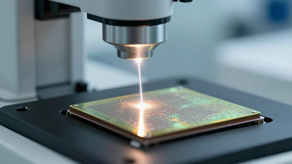
- •MIT and Oak Ridge moved 10,000 atoms in minutes at room temperature
- •Generated >40,000 quantum defects in under 40 minutes
- •Technique works in a 13‑nm‑thick chromium sulfide bromide crystal
- •Operates without high‑vacuum or cryogenic conditions
- •Potential to accelerate quantum‑device manufacturing and nanofabrication
Pulse Analysis
The MIT/Oak Ridge achievement marks a turning point for atomic‑scale engineering, shifting the field from a laboratory curiosity to a potentially manufacturable process. Historically, single‑atom manipulation required scanning tunneling microscopes operating at near‑absolute zero, limiting throughput and raising costs. By leveraging high‑speed electron‑beam algorithms, the researchers have compressed a task that once took days into a matter of minutes, effectively redefining the economics of defect engineering.
From a competitive standpoint, the breakthrough could compress the lead time for companies developing solid‑state qubits. Firms that have relied on stochastic defect generation may now face pressure to adopt deterministic placement to stay ahead in coherence times and error rates. Moreover, the room‑temperature capability lowers the barrier to entry for smaller players, potentially democratizing access to quantum‑grade materials and spurring a wave of niche startups focused on custom defect arrays.
Looking ahead, the key challenge will be scaling the method from a laboratory wafer to full‑size production substrates. Beam stability, throughput, and integration with existing lithography pipelines will determine whether the technology moves from proof‑of‑concept to a commercial workhorse. If those hurdles are cleared, we could see a cascade of new products—quantum sensors embedded in smartphones, ultra‑high‑resolution displays, and magnetic memory with atomically engineered anisotropy—within the next five years. The next milestone will likely be a pilot line demonstration that couples the electron‑beam system with standard semiconductor fab tools, a step that could unlock billions in market opportunity.
MIT and Oak Ridge Demonstrate Room‑Temp Manipulation of 10,000 Atoms in Minutes
Comments
Want to join the conversation?
Loading comments...