MIT’s ‘Implosion Carving’ Shrinks 3D Photonic Devices 2,000‑Fold for Visible‑Light Computing
Why It Matters
The ability to fabricate sub‑100 nm 3D photonic structures opens a practical path toward visible‑light optical processors, a class of devices that could dramatically cut the energy footprint of high‑performance computing. By overcoming the resolution barrier that has hampered 3D photonic integration, MIT’s implosion carving technique could accelerate research in optical neural networks, ultrafast imaging, and on‑chip light‑based communication. Moreover, the method’s reliance on hydrogel chemistry suggests a relatively low‑cost, scalable route compared with expensive electron‑beam facilities, potentially democratizing access to advanced nanophotonic manufacturing. Beyond computing, the technique may impact fields that require precise light manipulation at the nanoscale, such as biosensing, quantum optics, and photonic metamaterials. The convergence of nanofabrication, materials science, and optical engineering embodied in implosion carving exemplifies the interdisciplinary breakthroughs that drive the broader nanotech ecosystem forward.
Key Takeaways
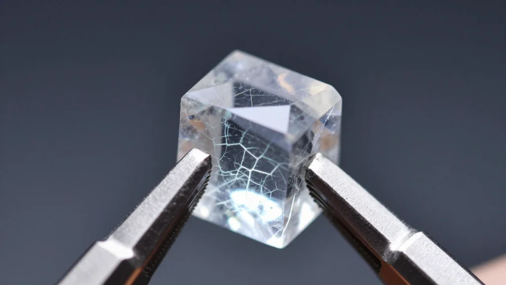
- •MIT’s implosion carving shrinks 3D hydrogel structures to 1/2,000 of their original volume, achieving <100 nm features.
- •Prototype device performed a digit‑classification task, proving functional optical computation.
- •Technique overcomes resolution limits of two‑photon lithography and electron‑beam lithography for 3D visible‑light structures.
- •Potential to enable energy‑efficient optical processors that could reduce data‑center power consumption.
- •Senior authors include Peter So (MIT LBCR director) and Edward Boyden (Howard Hughes investigator).
Pulse Analysis
Implosion carving arrives at a moment when the semiconductor industry is confronting the physical limits of Moore’s law. Optical computing has long been touted as a power‑saving alternative, but the lack of a manufacturable 3D platform for visible wavelengths has kept it in the research realm. MIT’s method flips that narrative by turning a bulk‑scale photopatterning step into a nanoscale precision tool, effectively decoupling feature size from the initial lithography resolution. This could compress development timelines dramatically, allowing startups and established chipmakers to prototype photonic circuits without the multi‑million‑dollar electron‑beam infrastructure.
Historically, breakthroughs in nanofabrication—such as the advent of deep‑UV lithography and later extreme‑UV—have been catalysts for new device generations. Implosion carving may play a similar role for photonics, especially as data‑intensive AI workloads demand ever‑greater bandwidth and lower latency. By enabling true 3D architectures that operate at visible wavelengths, the technique could support dense waveguide routing, on‑chip interferometry, and even integrated light‑based logic gates that are impossible with planar silicon photonics alone.
Looking ahead, the key to commercial impact will be integration. If MIT can partner with foundries to embed hydrogel‑based shrink steps into existing process flows, the barrier to entry for optical chips will fall sharply. Conversely, challenges such as material durability, thermal stability, and alignment with electronic control layers could slow adoption. Investors should watch for pilot production runs and collaborations with photonic foundries, as those milestones will signal whether implosion carving moves from a laboratory curiosity to a cornerstone of the next nanotech manufacturing paradigm.
MIT’s ‘Implosion Carving’ Shrinks 3D Photonic Devices 2,000‑Fold for Visible‑Light Computing
Comments
Want to join the conversation?
Loading comments...