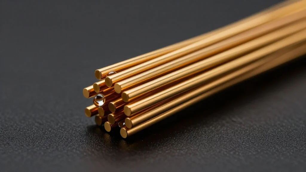
MIT‑Tokyo Team Boosts Carbon Nanotube Conductivity to Within 15% of Copper

Companies Mentioned
Why It Matters
Closing the conductivity gap between carbon nanotubes and copper could unlock lighter, more flexible wiring solutions for sectors where mass and corrosion are critical constraints, such as aerospace, wearable health monitors, and harsh‑environment telecommunications. By demonstrating a dopant that retains performance under elevated temperature and humidity, the MIT‑Tokyo team addresses a long‑standing reliability barrier that has kept CNTs on the periphery of commercial adoption. Beyond specific applications, the breakthrough signals a broader shift in nanomaterials engineering: the ability to fine‑tune electronic transport through molecular coatings may accelerate the integration of other low‑dimensional conductors, like graphene ribbons or transition‑metal dichalcogenide nanowires, into existing manufacturing pipelines. If the scaling challenges are solved, the industry could see a new class of hybrid interconnects that combine the best of metal and nanomaterial properties, reshaping supply chains and design standards for next‑generation electronics.
Key Takeaways
- •PEI dopant raises metallic CNT bundle conductivity by 40% to 5.8×10⁷ S/m.
- •Conductivity now within 15% of annealed copper at room temperature.
- •Stability test shows 92% conductivity retention after 500 hours at 85 °C.
- •IBM pilot line reports 17% yield loss during thermocompression lamination.
- •MIT aims for 10‑meter CNT ribbons by early 2027; Tokyo team targets 1,000‑hour thermal cycling.
Pulse Analysis
The MIT‑Tokyo breakthrough arrives at a moment when the semiconductor industry is wrestling with the physical limits of copper interconnects. As feature sizes shrink below 10 nm, copper’s resistivity climbs due to surface scattering, prompting a search for alternatives that can sustain high current densities without electromigration. Doped CNTs, with their quasi‑ballistic transport, have long been touted as a theoretical solution, but practical implementation has been hampered by inconsistent doping and poor environmental stability. The PEI coating not only delivers a measurable conductivity jump but also demonstrates a realistic path to durability, which could revive interest from chipmakers that have previously shelved CNT programs.
Nevertheless, the commercial calculus remains complex. Scaling meter‑long, high‑purity metallic CNT fibers demands new synthesis equipment, tighter quality control, and substantial capital investment. Existing copper infrastructure—foundries, plating lines, and supply chains—offers economies of scale that CNTs cannot yet match. The real market entry points are likely to be high‑value, low‑volume segments where weight savings translate directly into performance gains, such as satellite tethers or aerospace wiring harnesses. In those niches, the cost premium of a novel nanomaterial can be justified by the reduction in launch mass and the elimination of corrosion‑related maintenance.
Looking ahead, the next decisive factor will be integration. If IBM’s process adaptations and the upcoming MIT‑Tokyo pilot runs prove that PEI‑doped CNTs can survive standard PCB fabrication steps, the technology could cascade into broader electronics manufacturing. Conversely, if alignment and adhesion issues persist, the industry may revert to hybrid approaches—using CNTs for specific functions like flexible interposers while retaining copper for bulk routing. Either way, the announcement re‑energizes the nanotech sector, signaling that the long‑awaited marriage of nanomaterials and mass‑production is inching closer to reality.
MIT‑Tokyo Team Boosts Carbon Nanotube Conductivity to Within 15% of Copper
Comments
Want to join the conversation?
Loading comments...