Monolithic 3D Nanoelectrode Arrays on CMOS Circuitry for Scalable, High‐Resolution Neural Recording
•March 2, 2026
0
Why It Matters
The HD‑NEA delivers unprecedented recording density and signal fidelity, enabling more detailed neural circuit analysis and accelerating preclinical drug testing. Its CMOS compatibility also opens a path toward cost‑effective, large‑scale neurotechnology deployment.
Key Takeaways
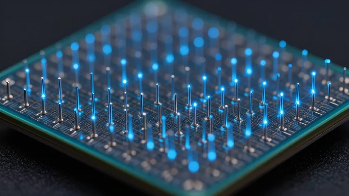
- •26,400 vertical nanoelectrodes integrated on CMOS wafer.
- •Low‑temperature (<400 °C) post‑fabrication preserves circuit function.
- •Spike amplitude and SNR dramatically higher than planar arrays.
- •Detects diverse waveforms, including dendritic signals, without electroporation.
- •Scalable platform for neuroscience, drug screening, and brain‑machine interfaces.
Pulse Analysis
The quest for detailed brain activity maps has driven rapid advances in electrophysiology. Traditional planar microelectrode arrays offer limited spatial resolution and often require invasive procedures or electroporation to achieve sufficient signal quality. As neuroscience pushes toward single‑cell and subcellular insights, the industry demands interfaces that combine nanoscale sensitivity with the ability to record from thousands of sites simultaneously. This pressure has spurred research into three‑dimensional nanostructured electrodes that can bring recording sites closer to neuronal membranes, thereby enhancing signal fidelity without compromising cell health.
The study introduces a monolithically integrated high‑density nanoelectrode array (HD‑NEA) built directly on commercial CMOS chips. Using a low‑temperature (<400 °C) post‑fabrication process, vertical nanowire electrodes are added to the back‑end‑of‑line, preserving circuit functionality across 4‑inch wafers. The resulting platform hosts 26,400 three‑dimensional nanoelectrodes with uniform performance and high manufacturing yield. In vitro tests with cortical cultures show spike amplitudes and signal‑to‑noise ratios far exceeding those of planar electrodes, while also capturing diverse waveforms, including putative dendritic signals, without electroporation.
These results position the HD‑NEA as a scalable, CMOS‑compatible bridge between nanobioelectronics and large‑scale neural recording. For drug discovery, the ability to monitor thousands of neurons with sub‑micron precision could accelerate toxicity screening and mechanism‑of‑action studies. In brain‑machine interface research, the dense, high‑fidelity data stream may enable more nuanced decoding of motor intent and sensory feedback. As the semiconductor industry continues to push wafer‑scale integration, further reductions in electrode pitch and power consumption are likely, paving the way for implantable versions that retain the same performance advantages.
Monolithic 3D Nanoelectrode Arrays on CMOS Circuitry for Scalable, High‐Resolution Neural Recording
0
Comments
Want to join the conversation?
Loading comments...