Most Lab Testing Quietly Inflates 2D Transistor Performance, Research Reveals
•February 27, 2026
0
Why It Matters
Inflated performance metrics mislead investors and engineers, potentially derailing the roadmap for integrating 2D materials into future semiconductor technologies.
Key Takeaways
- •Back‑gate architecture introduces contact gating effect
- •Contact gating can double or sextuple performance
- •Real‑world devices cannot use back‑gate design
- •Symmetric dual‑gate test isolates contact gating impact
- •Findings call for revised benchmarking standards
Pulse Analysis
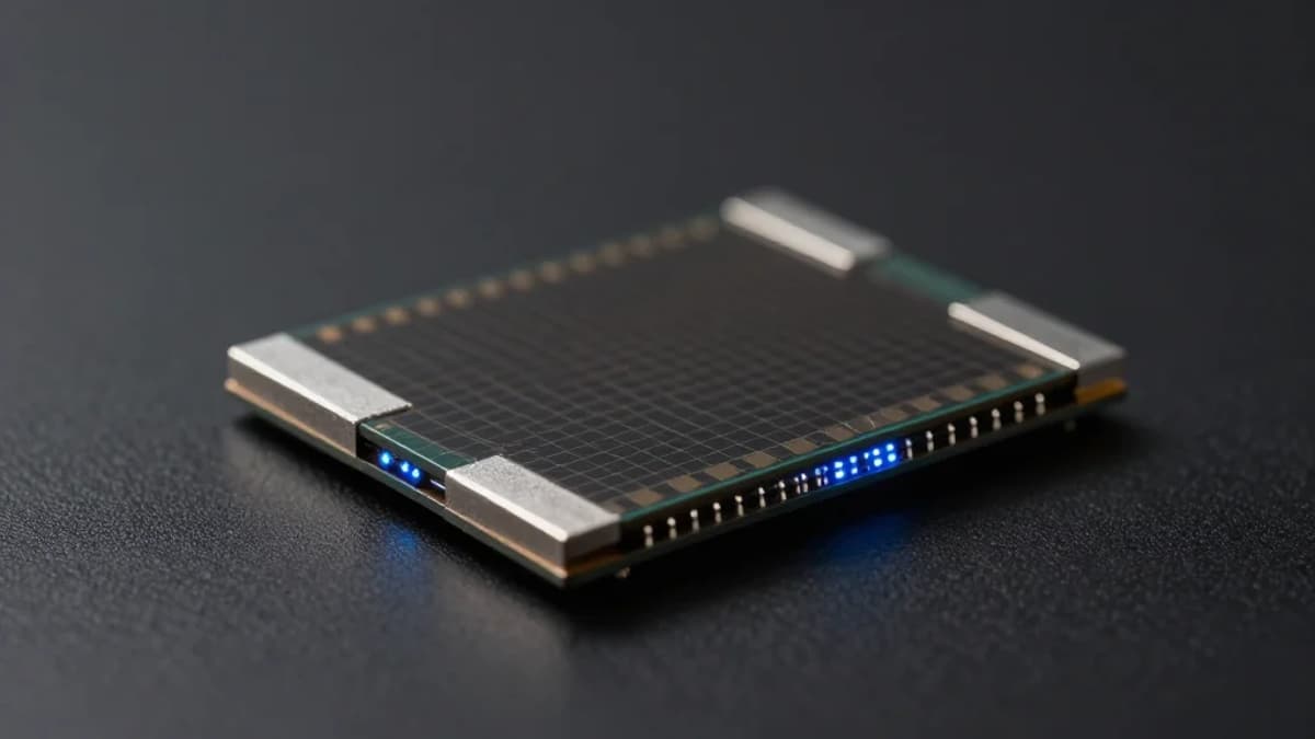
Two‑dimensional semiconductors have been hailed as the next frontier beyond silicon, offering atom‑thin channels that could keep Moore’s Law alive. Yet most academic groups rely on a back‑gated test platform because it simplifies fabrication and speeds up data collection. In that configuration the substrate gate unintentionally lowers contact resistance, a side effect known as contact gating, which makes the transistor appear faster and more efficient than it would be in a production‑grade layout.
Duke’s electrical engineering team tackled the bias by designing a symmetric dual‑gate transistor, where a top gate mirrors the conventional back gate. This architecture lets researchers toggle contact gating on and off while keeping every other variable constant. Their measurements revealed that, at a 50 nm channel and 30 nm contacts, the back‑gate setup could amplify current drive by up to six times compared with a realistic top‑gate‑only design. As devices shrink, contacts dominate overall behavior, so the distortion grows rather than diminishes, exposing a systemic overestimation in the literature.
The implications are immediate for both academia and industry. Venture capital and R&D budgets that have been allocated based on optimistic lab figures may need reassessment, and semiconductor roadmaps must incorporate more stringent, device‑level testing standards. Future work will push contact dimensions below 15 nm and explore alternative metals to truly gauge the intrinsic limits of 2D channels. By aligning measurement practices with manufacturable architectures, the field can better determine whether 2D materials will complement or replace silicon in next‑generation processors.
Most lab testing quietly inflates 2D transistor performance, research reveals
0
Comments
Want to join the conversation?
Loading comments...