Nanohole Arrays Boost Quantum Light Source Brightness 130‑Fold at Room Temperature
Why It Matters
The ability to generate bright, stable quantum light at room temperature removes a major barrier to scaling quantum communication and computing hardware. Current quantum‑dot sources require cryogenic cooling, inflating cost and limiting deployment to specialized labs. By leveraging nanohole‑mediated exciton confinement, the new approach promises mass‑manufacturable photonic components that can be integrated directly onto silicon platforms, accelerating the rollout of quantum‑secure links and photonic quantum processors. Beyond communications, the technique could impact quantum sensing and metrology, where high‑efficiency single‑photon sources improve measurement precision. The convergence of 2D semiconductor fabrication with established wafer‑scale processes also opens opportunities for cross‑industry collaboration, linking nanophotonics, semiconductor manufacturing, and quantum information science.
Key Takeaways
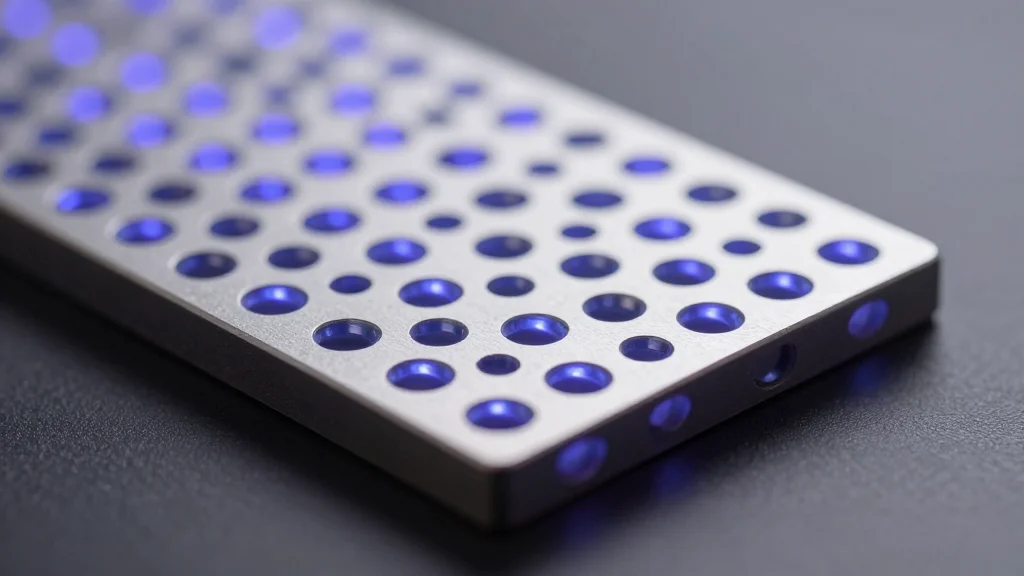
- •130‑fold increase in luminescence efficiency achieved with 500 nm nanohole arrays
- •Exciton confinement efficiency measured at ~98% at room temperature
- •Research published in Science Advances on March 13, 2026
- •Team led by IBS associate director Seo Young‑Duk and POSTECH professor Park Kyoung‑Duck
- •Potential for mass‑production using standard semiconductor wafer processes
Pulse Analysis
The nanohole breakthrough arrives at a moment when the quantum‑technology market is racing to overcome the cost and complexity of cryogenic systems. Historically, quantum light sources have been confined to laboratory settings because exciton recombination rates drop sharply at ambient temperatures. By engineering a nanostructured potential well that corrals excitons with near‑perfect efficiency, the IBS‑POSTECH team sidesteps the thermal decoherence that has hampered prior designs.
From a competitive standpoint, the result positions South Korea as a serious contender in the global quantum photonics race, traditionally dominated by U.S. and European labs. The use of 2D semiconductors—materials already being explored for next‑generation transistors—means the technology can piggyback on existing supply chains, shortening time‑to‑market. Companies that have invested in silicon‑photonic integration may find a ready‑made quantum light source that plugs into their platforms without redesigning cooling infrastructure.
Looking ahead, the key challenge will be translating the laboratory‑scale nanohole patterning into high‑throughput lithography compatible with foundry standards. If the team can shrink the hole diameter below 200 nm while preserving confinement, deterministic single‑photon emission rates suitable for error‑corrected quantum computing could be realized. Such progress would not only validate the scientific premise but also unlock a new class of quantum devices that are both affordable and scalable, potentially reshaping the economics of the emerging quantum ecosystem.
Nanohole Arrays Boost Quantum Light Source Brightness 130‑Fold at Room Temperature
Comments
Want to join the conversation?
Loading comments...