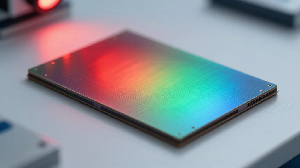
Nanoscale Device Converts Wasted Infrared Light Into Usable Energy
Key Takeaways
- •8.2% photon‑conversion efficiency sets new benchmark for solid‑state upconversion
- •Device operates in thin film, compatible with semiconductor manufacturing processes
- •Converting infrared to visible light can lift silicon solar panel efficiency
- •Applications span solar energy, infrared sensing, 3D printing, medical therapies
Pulse Analysis
The breakthrough addresses a core limitation in photonics: the inability to harvest low‑energy infrared photons that normally pass through silicon cells or dissipate as heat. By engineering molecular structures that localize excitons and enable solid‑state sensitized triplet‑fusion upconversion, the UNSW team achieved an 8.2% conversion rate, rivaling the best liquid‑phase systems while eliminating the need for cumbersome solvents. This solid‑state approach simplifies integration with existing semiconductor lines, reducing production costs and enhancing durability for real‑world deployment.
For the solar industry, the implication is immediate. Conventional silicon panels convert roughly 20% of incident sunlight, leaving a large fraction of infrared radiation untapped. Embedding the upconversion film onto or beneath photovoltaic layers could shift a portion of that infrared spectrum into the visible range, where silicon’s quantum efficiency is higher. Early modeling suggests potential gains of 1‑2 percentage points in overall panel efficiency, a meaningful improvement given the scale of global solar capacity. Beyond photovoltaics, the technology offers a low‑cost route to enhance infrared sensors, enabling clearer night‑vision imaging and more sensitive environmental monitoring.
Commercialization prospects are bolstered by the device’s compatibility with standard wafer‑scale fabrication, positioning it for rapid adoption in sectors ranging from volumetric 3D printing to biomedical therapies that require deeper tissue light penetration. As the market for renewable energy and advanced photonic devices expands, investors are likely to view solid‑state upconversion as a strategic differentiator. Continued scaling, coupled with integration into existing manufacturing pipelines, could see the technology entering pilot projects within the next two to three years, driving both efficiency gains and new product categories.
Nanoscale device converts wasted infrared light into usable energy
Comments
Want to join the conversation?