Nanoscience at the Centre of Optical Computing
•January 20, 2026
0
Companies Mentioned
Why It Matters
By cutting the energy per operation dramatically, nanophotonic optical processors can alleviate data‑center power constraints and unlock new AI performance levels. Their adoption will reshape the compute ecosystem, adding a high‑efficiency, photonic layer alongside traditional silicon.
Key Takeaways
- •Nanophotonics reduces AI compute energy by orders of magnitude
- •Plasmonic modulators face loss and thermal challenges at scale
- •Quantum‑dot lasers enable dense optical interconnects for data centers
- •Metasurfaces perform on‑chip matrix multiplication, shrinking optics
- •Scalable nanofabrication mirrors SOI's historic manufacturing breakthrough
Pulse Analysis
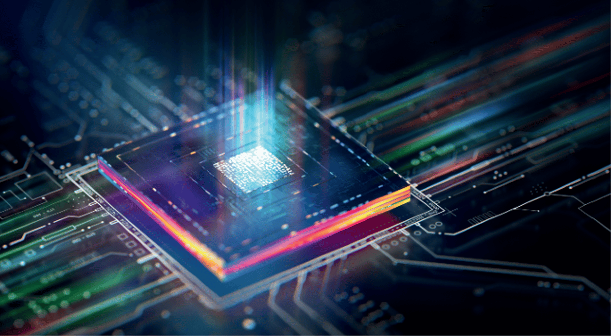
The surge in AI workloads has turned power consumption into a strategic constraint, prompting a search for alternatives to silicon transistors. Optical computing, by processing data with photons rather than electrons, can deliver terabit‑per‑second bandwidth while dissipating a fraction of the energy required by conventional ASICs. Recent nanophotonic breakthroughs—particularly in high‑Q photonic crystals and ultra‑compact metasurfaces—allow linear algebra operations to be executed directly in the optical domain, delivering performance measured in tens of tera‑operations per second per watt (TOPS/W). This shift promises to decouple AI scaling from the thermal ceiling that now limits data‑center expansion. At the material level, several nanostructured platforms are converging to make on‑chip light processing feasible. Plasmonic interfaces confine fields to sub‑100‑nm gaps, enabling electro‑optic modulation speeds beyond silicon’s limits, yet they suffer from metal‑induced loss and heat that must be mitigated through novel designs. Quantum‑dot lasers provide electrically pumped, wavelength‑tunable sources that can be monolithically integrated onto silicon, accelerating optical interconnect adoption. Metasurfaces encode mathematical transforms in patterned resonators, collapsing free‑space optics into millimetre‑scale chips. Meanwhile, phase‑change alloys such as Ge‑Sb‑Te introduce non‑volatile optical weights, allowing learning rules to be stored directly in photonic circuits. Scaling these concepts from laboratory demos to volume production hinges on advances in nanofabrication that echo the Smart‑Cut revolution for silicon‑on‑insulator wafers. Techniques like deep‑UV lithography, nanoimprint, and wafer‑bonded heterogeneous integration are already delivering the sub‑50‑nm tolerances required for dense photonic routing. Companies such as Vector Photonics, Quintessent, and Neurophos are building supply chains around these processes, positioning optical accelerators as a complementary tier to CMOS in future heterogeneous compute stacks. As energy‑aware AI proliferates, the convergence of nanoscience and mass manufacturing will likely define the next competitive edge in high‑performance computing.
Nanoscience at the centre of optical computing
0
Comments
Want to join the conversation?
Loading comments...