New 4D-STEM Method Isolates Atomic Structures From Clustered Nanocrystals
•March 4, 2026
0
Why It Matters
The technique unlocks atomic‑scale insight for nanomaterials that were inaccessible to traditional X‑ray or electron diffraction, accelerating discovery in energy, pharma, and materials engineering.
Key Takeaways
- •4D‑STEM uses nanometer electron beam, records diffraction per probe.
- •Virtual apertures isolate individual nanocrystals within clusters.
- •4D Camera captures 87,000 frames per second, streams to Perlmutter.
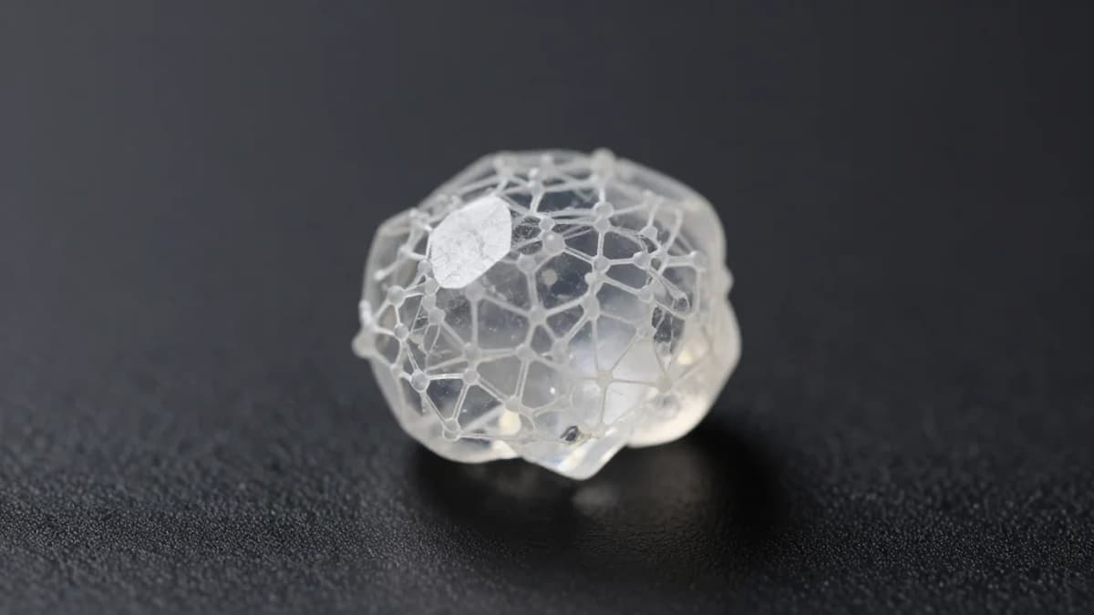
- •Method solved UiO‑66 MOF structure from 300 nm crystals.
- •Enables crystallography of previously inaccessible nanoscale materials.
Pulse Analysis
The new 4D‑STEM protocol pushes electron microscopy beyond conventional limits by shrinking the probe to a few nanometers and capturing a full diffraction pattern at each raster point. Unlike microcrystal electron diffraction, which relies on a broad beam and physical apertures, the virtual aperture software lets researchers draw custom masks around the most informative regions of a sample. This pixel‑by‑pixel selection dramatically improves signal quality and makes it possible to extract crystallographic data from tangled nanocrystal aggregates.
At the heart of the workflow is the 4D Camera, a detector capable of recording 87,000 frames per second—roughly 1,500 times faster than a typical broadband internet connection. The massive data stream is routed directly to Berkeley Lab’s Perlmutter supercomputer, where specialized compression algorithms reduce terabytes of sparse frames in real time. By adapting software originally built for X‑ray crystallography, the team can process electron‑derived diffraction sets with unprecedented speed and accuracy, turning raw microscope output into actionable structural models.
The broader impact reaches across multiple sectors. Metal‑organic frameworks like UiO‑66, which underpin next‑generation gas storage, catalysis, and drug‑delivery platforms, often form only as sub‑micron crystals that defy traditional analysis. With 4D‑STEM, scientists can now resolve their atomic lattices, informing design cycles and accelerating commercialization. As the method matures, it promises to democratize high‑resolution structure determination for any nanomaterial, from quantum dots to battery electrodes, reshaping research pipelines in both academia and industry.
New 4D-STEM method isolates atomic structures from clustered nanocrystals
0
Comments
Want to join the conversation?
Loading comments...