New Global Standard Set for Testing Graphene's Single-Atom Thickness
•January 13, 2026
0
Why It Matters
A universally accepted testing standard removes quality ambiguity, allowing graphene to move from laboratory curiosity to reliable component in automotive, electronics, and consumer‑goods supply chains.
Key Takeaways
- •Global TEM protocol standardizes graphene monolayer measurement
- •ISO/TS 21356‑2 incorporates the new protocol
- •15 labs validated method, reducing uncertainty
- •Commercial TEM services offered via Royce Institute
- •Enables reliable integration of graphene in products
Pulse Analysis
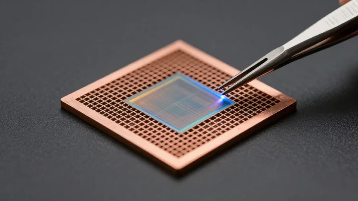
Graphene’s promise has long been hampered by a lack of consistent quality metrics. While its extraordinary electrical conductivity, strength, and flexibility are well documented, manufacturers have struggled to confirm that a given batch truly consists of a single‑atom layer. Without a reliable, repeatable test, supply chains face risk of performance shortfalls, warranty claims, and slowed adoption. The new TEM‑based protocol addresses this gap by delivering quantifiable thickness data with clearly defined uncertainty bounds, turning graphene from a speculative material into a certifiable commodity.
The inter‑laboratory study coordinated by Manchester leveraged the expertise of fifteen leading labs across Europe, Asia, and North America. Researchers systematically compared electron diffraction patterns, refined calibration routines, and codified best‑practice sample preparation steps. Their findings, now embedded in ISO/TS 21356‑2, provide a clear, step‑by‑step guide that can be implemented in standard TEM facilities. Importantly, the protocol was designed for scalability: it does not require exotic equipment beyond a conventional high‑resolution TEM, and the accompanying uncertainty model enables manufacturers to report confidence levels alongside thickness measurements.
For industry, the standard unlocks a cascade of opportunities. Automotive firms can certify graphene‑reinforced composites for lightweight chassis, while semiconductor manufacturers gain a reliable path to integrate graphene interconnects into next‑generation chips. The partnership with the Royce Institute further democratizes access, offering commercial testing for companies lacking in‑house TEM capabilities. As the ISO specification gains traction, investors and supply‑chain managers will have a concrete benchmark to assess risk, accelerating capital deployment into graphene‑enabled products and fostering a new wave of innovation across sectors.
New global standard set for testing graphene's single-atom thickness
0
Comments
Want to join the conversation?
Loading comments...