New Graphene-Based Laser Transfer Method Could Advance Flexible Electronics
•January 16, 2026
0
Why It Matters
The method removes a major bottleneck in flexible electronics manufacturing by simplifying alignment and boosting yield, paving the way for cost‑effective, high‑volume production of advanced displays and IoT devices.
Key Takeaways
- •SALT uses TCGC for directional heat conduction.
- •No precise laser‑to‑die alignment required.
- •Transfer accuracy under 5 µm with 30% beam offset.
- •Reversible adhesion switchability reaches ~650 %.
- •Supports 100 µm‑1 mm chips on 3D surfaces.
Pulse Analysis
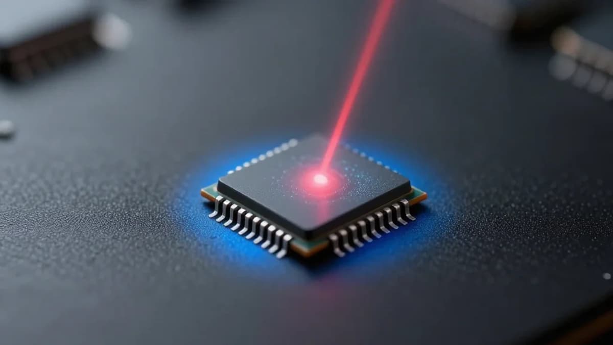
Flexible electronics have long been hampered by the difficulty of placing tiny components on non‑planar surfaces with sub‑micron accuracy. Traditional laser‑based pick‑and‑place systems demand meticulous alignment, driving up equipment costs and reducing throughput. The newly reported self‑aligned laser transfer (SALT) sidesteps these constraints by embedding a thermal conductivity gradient carbon (TCGC) layer directly onto the transfer stamp. This engineered gradient, featuring a high‑conductivity graphene skin atop low‑conductivity amorphous carbon, channels laser‑induced heat in a controlled manner, creating a uniform temperature field that releases chips precisely where needed.
The core advantage of SALT lies in its programmable, high‑precision microchip handling. By converting asymmetric light intensity into even heat distribution, the system tolerates significant beam misalignment—up to a 30 % offset—while still achieving placement errors below five micrometers. Performance metrics such as a reversible adhesion switchability of roughly 650 % and a rapid 30 ms response time demonstrate that the process can keep pace with high‑volume manufacturing demands. Moreover, the technique accommodates a broad size range, from 100 µm to 1 mm, and works on curved substrates, opening new design possibilities for wearable sensors, conformal displays, and three‑dimensional circuitry.
Industry implications are substantial. The ability to batch‑transfer RGB MicroLEDs without pre‑planned scanning paths could dramatically lower the cost and complexity of full‑color MicroLED displays, a market segment poised for rapid growth. Additionally, the SALT approach aligns with the broader push toward scalable, low‑temperature processes compatible with polymeric and glass‑based flexible platforms. As manufacturers seek to meet the escalating demand for lightweight, bendable, and high‑resolution electronics, this graphene‑enabled laser transfer method offers a compelling pathway to bridge laboratory breakthroughs with commercial production lines.
New graphene-based laser transfer method could advance flexible electronics
0
Comments
Want to join the conversation?
Loading comments...