NY Creates Starts Installing First High‑NA EUV Lithography Tool at Albany
Companies Mentioned
Why It Matters
The installation of a high‑NA EUV lithography system in New York marks a decisive step toward domesticizing the most advanced chip‑making technology, which has been largely confined to a few overseas locations. By embedding this capability within the Albany Nanotech Complex, the United States gains a research hub that can accelerate the development of sub‑3‑nanometer nodes, essential for next‑generation processors, AI accelerators, and high‑performance memory. The $10 billion public‑private investment also demonstrates a model for scaling semiconductor R&D infrastructure without relying solely on federal funds, potentially inspiring similar initiatives in other regions. Beyond technical advances, the project is a catalyst for economic development. The center is expected to create high‑skill jobs, attract talent, and stimulate ancillary industries such as equipment manufacturing, materials supply, and advanced packaging. In the broader geopolitical context, bolstering U.S. EUV capacity helps mitigate supply chain vulnerabilities and counters the strategic advantage that rivals, particularly China, seek in semiconductor technology. The Albany initiative thus serves both as an innovation engine and a strategic asset for national security.
Key Takeaways
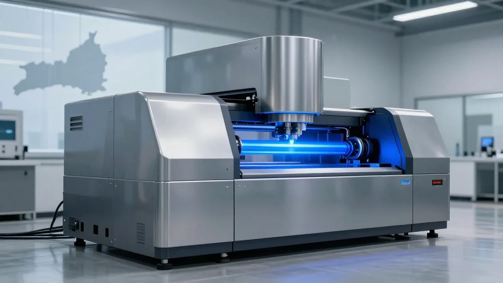
- •Installation of ASML's high‑NA EUV lithography system at Albany Nanotech Complex will begin in the coming months.
- •The project is part of a $10 billion partnership: $9 billion from industry, $1 billion from Empire State Development.
- •First‑light operation is targeted for before the end of 2026, enabling sub‑3‑nm research.
- •Key participants include Governor Kathy Hochul, Empire State Development’s Hope Knight, Senator Charles Schumer, and NY Creates CEO Dave Anderson.
- •The center aims to keep the U.S. ahead of China in advanced chip manufacturing and generate high‑quality jobs in upstate New York.
Pulse Analysis
The Albany high‑NA EUV installation is more than a regional milestone; it signals a shift in how the United States approaches cutting‑edge semiconductor R&D. Historically, the U.S. has relied on a handful of legacy fabs and foreign EUV suppliers to push node scaling. By embedding a high‑NA tool—a technology that can print features below 10 nm with unprecedented fidelity—directly within a research complex, New York is creating a feedback loop where academic insight, industry engineering, and government policy converge. This model reduces the lag between discovery and production, potentially shortening the time to market for next‑generation chips.
From a competitive standpoint, the move counters the concentration of high‑NA EUV capacity in the Netherlands (ASML’s home) and Taiwan’s TSMC. While ASML remains the sole supplier of such machines, the location of the tool determines where the expertise and data accumulate. Albany’s proximity to leading U.S. chip designers (IBM, Micron) and equipment manufacturers (Applied Materials, Tokyo Electron) creates a domestic ecosystem that can iterate faster on process integration, mask design, and materials science. The $9 billion industry commitment underscores that private players see tangible ROI in co‑locating with the tool, anticipating that breakthroughs will translate into commercial patents and product differentiation.
Looking forward, the success of the Albany center will likely influence future CHIPS & Science allocations. If the first‑light demonstration yields measurable improvements in patterning accuracy and throughput, policymakers may justify additional federal grants to replicate the model in other innovation corridors. Conversely, any technical setbacks could reinforce the argument for a more cautious, phased rollout of high‑NA EUV across the country. Either way, the Albany project sets a benchmark for public‑private collaboration in nanotech infrastructure, and its outcomes will shape the strategic roadmap for U.S. semiconductor leadership over the next decade.
NY Creates Starts Installing First High‑NA EUV Lithography Tool at Albany
Comments
Want to join the conversation?
Loading comments...