Paragraf Launches Mass‑produced Graphene Transistors From New Huntingdon Foundry
Companies Mentioned
Why It Matters
The PMF2000 launch demonstrates that graphene can be integrated into high‑volume semiconductor manufacturing, a hurdle that has limited commercial adoption for years. By delivering a consistent, contamination‑free graphene layer at wafer scale, Paragraf reduces the performance‑to‑cost gap that has kept graphene sensors in niche labs. This could accelerate the deployment of ultra‑sensitive detectors in healthcare, where early disease markers demand higher resolution, and in agriculture, where real‑time monitoring of soil nutrients can improve yields. Moreover, the establishment of a dedicated graphene foundry signals a shift in the semiconductor supply chain. Traditional silicon fabs have been reluctant to invest in graphene tooling due to uncertain demand. Paragraf’s model—combining a specialized facility with an online marketplace—offers a template for other niche material manufacturers to achieve economies of scale without relying on legacy fabs. If successful, the approach could spur a broader ecosystem of graphene‑enabled components, from flexible displays to quantum‑ready devices.
Key Takeaways
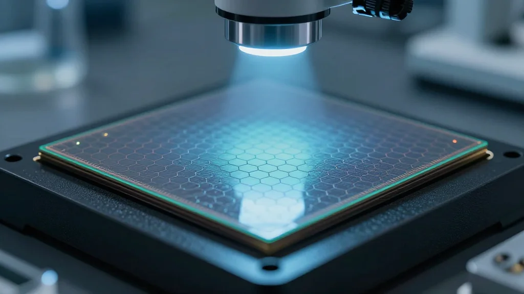
- •Paragraf launches PMF2000 GFET, the first mass‑produced graphene transistor from its Huntingdon facility
- •Huntingdon plant is the first dedicated graphene foundry, featuring a 6‑inch wafer line for contamination‑free graphene layers
- •PMF2000 targets molecular‑sensing applications in healthcare, agriculture, chemical processing, and industrial monitoring
- •CEO Dr Simon Thomas says the launch proves graphene‑on‑silicon can deliver high‑performance, scalable semiconductors
- •Transistors are sold via Paragraf’s online store, with a discovery kit to speed developer adoption
Pulse Analysis
Paragraf’s move to commercial‑scale graphene production arrives at a moment when the sensor market is hungry for higher sensitivity and lower power consumption. Traditional silicon sensors are approaching physical limits, especially for detecting low‑concentration biomolecules. Graphene’s atomically thin lattice offers a quantum‑level interface that can translate minute chemical changes into measurable electrical signals. By marrying this material with a silicon substrate, Paragraf sidesteps the need for entirely new manufacturing ecosystems, leveraging existing fab expertise while adding a thin graphene overlay.
Historically, graphene’s promise has been hampered by inconsistent material quality and the high cost of small‑batch processes. The Huntingdon facility’s focus on large‑wafer production directly addresses these pain points, potentially driving down per‑unit costs and improving yield. If Paragraf can sustain volume shipments, it may force larger foundries—such as TSMC or GlobalFoundries—to consider dedicated graphene lines, accelerating industry‑wide adoption.
Looking ahead, the real test will be market traction. Early adopters in biotech and agritech are likely to pilot the PMF2000, but broader uptake will depend on demonstrated reliability, supply chain stability, and clear ROI compared with silicon alternatives. Paragraf’s online store and discovery kit lower the barrier for developers, but scaling beyond niche pilots will require partnerships with OEMs and system integrators. Should those relationships materialize, the company could capture a sizable slice of the projected $30 billion sensor market by 2030, positioning graphene as a mainstream semiconductor material rather than a laboratory specialty.
Paragraf launches mass‑produced graphene transistors from new Huntingdon foundry
Comments
Want to join the conversation?
Loading comments...