Polish Researchers Trap Infrared Light in 40‑nm Film, 1,000× Thinner Than Hair
Why It Matters
Confining light in a film thinner than a human hair overturns a long‑standing limitation in nanophotonics, where the wavelength of light set a lower bound on device dimensions. By demonstrating that MoSe₂ can slow infrared photons enough to be trapped in a 40‑nm layer, the work opens a route to ultra‑compact photonic circuits that operate at speeds far beyond electronic transistors. This could accelerate the transition to optical interconnects in data centers, reduce power consumption, and enable new sensing modalities that rely on strong light‑matter interaction in a minimal footprint. Beyond immediate applications, the breakthrough showcases the value of layered transition‑metal dichalcogenides as a new class of photonic materials. Their semiconductor nature, combined with high refractive index and nonlinear optical properties, positions them as versatile building blocks for future quantum‑photonic platforms, where controlling photons at the nanoscale is essential.
Key Takeaways
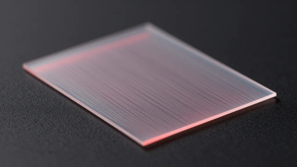
- •40 nm MoSe₂ sub‑wavelength grating traps infrared light, >1,000× thinner than hair
- •Refractive index slows light ~4.5× more than glass, enabling extreme miniaturization
- •Demonstrates strong third‑harmonic generation, converting infrared to visible blue
- •Collaboration among University of Warsaw, Łódź University of Technology, Warsaw University of Technology, Polish Academy of Sciences
- •Published in ACS Nano; potential to shrink photonic components for data‑center and sensing markets
Pulse Analysis
The 40‑nm MoSe₂ grating arrives at a moment when the semiconductor industry is confronting the physical limits of Moore's Law. Photonic integration has been touted as the next scaling lever, yet most on‑chip optical components still occupy hundreds of nanometers, limiting how densely they can be packed. By slashing the confinement layer to a few dozen nanometers, the Polish team not only proves a concept but also forces a re‑evaluation of design rules for photonic foundries. Companies such as Intel and IBM have invested heavily in silicon‑photonic transceivers; a MoSe₂‑based approach could complement or even replace silicon in the most size‑critical sections, especially where nonlinear conversion is required.
From a market perspective, the ability to generate visible light from infrared on the same chip could catalyze new product categories—compact spectrometers for environmental monitoring, point‑of‑care diagnostics, and secure quantum‑key‑distribution modules. The projected $800 billion photonics market will likely allocate a growing share to materials beyond silicon, and MoSe₂’s compatibility with existing thin‑film deposition processes lowers the barrier to entry for foundries. However, the path to volume production will hinge on reproducibility of the grating geometry and integration with CMOS, challenges that have stalled similar nanophotonic promises in the past.
Looking ahead, the next 12‑18 months will be critical. If the research group can demonstrate wafer‑scale fabrication and stable operation under industry‑standard testing, venture capital could flow into spin‑outs focused on MoSe₂ photonic components. Conversely, if scaling proves costly, the technology may remain a laboratory curiosity. Either way, the breakthrough sharpens the strategic focus on transition‑metal dichalcogenides as a cornerstone of the post‑electronic era.
Polish Researchers Trap Infrared Light in 40‑nm Film, 1,000× Thinner Than Hair
Comments
Want to join the conversation?
Loading comments...