POSTECH Team Demonstrates Ballistic Electron Transport in Copper Interconnects
Why It Matters
Ballistic electron transport in copper directly tackles two of the semiconductor industry's most pressing constraints: power density and signal latency. By enabling electrons to traverse interconnects with minimal scattering, chips can operate faster while dissipating less heat, extending the viability of Moore’s law beyond the current node limits. Moreover, because copper is already the standard interconnect material, the breakthrough sidesteps the costly retooling required for exotic alternatives, offering a more immediate path to commercial impact. The discovery also reshapes research priorities. Instead of focusing solely on new materials, engineers can now invest in crystal‑quality deposition techniques and surface engineering to unlock performance gains from existing metals. If the temperature barrier is overcome, the approach could become a cornerstone of future low‑power architectures, influencing everything from mobile processors to data‑center accelerators.
Key Takeaways
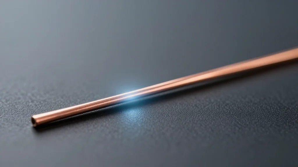
- •POSTECH-led team observed ballistic transport in copper interconnects 90 nm thick, 150 nm wide.
- •Negative bend resistance measured below –188 °C confirms collision‑free electron flow.
- •Single‑crystal copper film created via atomic sputtering epitaxy with 0.2 nm surface roughness.
- •Potential to reduce interconnect power loss by up to 30 % and improve signal speed.
- •Next steps include room‑temperature testing and integration into prototype chips by late 2026.
Pulse Analysis
The POSTECH breakthrough reintroduces copper as a contender in the race for ultra‑low‑power interconnects, a space that has been dominated by exotic two‑dimensional materials for the past decade. Historically, the industry’s focus shifted to graphene and carbon nanotubes after conventional metals hit a scattering ceiling. This research flips that narrative by showing that the scattering problem is not intrinsic to copper but rather a consequence of its polycrystalline microstructure. By engineering a single‑crystal film, the team effectively restores copper’s latent ballistic potential.
From a market perspective, the timing is critical. Semiconductor fabs are currently investing billions in advanced packaging, 3‑D stacking, and silicon‑photonic links to sidestep the thermal wall. A copper‑based ballistic solution could complement these strategies, offering a drop‑in upgrade that leverages existing deposition equipment with modest modifications. However, the low‑temperature requirement underscores a classic trade‑off: performance gains versus practical manufacturability. If the consortium can demonstrate ballistic behavior at or near room temperature, it would dramatically accelerate adoption, potentially reshaping the BEOL roadmap for the next five years.
Strategically, the result also signals a shift in research funding toward process‑centric innovations. Venture capital and government grants have increasingly favored novel material discovery; this success suggests that deep‑tech investors might now look to fund advanced epitaxy platforms and crystal‑growth tooling. The competitive landscape will likely see major foundries—TSMC, Samsung, Intel—testing similar ASE processes in parallel, sparking a new wave of patents around single‑crystal metal deposition. In the short term, the key question remains whether the ballistic effect can survive the thermal and mechanical stresses of real‑world chip operation. The answer will determine whether this discovery becomes a niche academic curiosity or a foundational technology for the next generation of energy‑efficient processors.
POSTECH Team Demonstrates Ballistic Electron Transport in Copper Interconnects
Comments
Want to join the conversation?
Loading comments...