Real-Time Microscopy Reveals How Semiconductor Nanowires Grow, and How Bismuth Seeds Can Speed Their Formation
Why It Matters
Real‑time insight into nucleation and growth lets manufacturers fine‑tune low‑cost, scalable nanowire synthesis, directly impacting performance and market adoption of next‑generation semiconductor technologies.
Key Takeaways
- •Liquid‑phase TEM visualized tellurium nucleation and nanowire branching.
- •Growth rates measured between 1 nm/s and 15 nm/s.
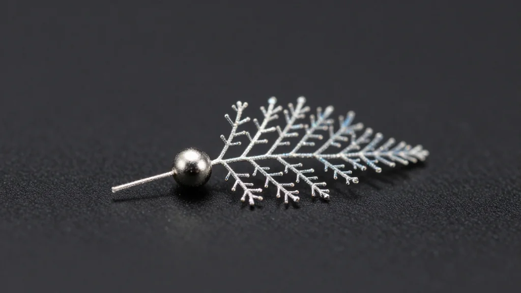
- •Bismuth seeds increase nucleation sites and promote fern‑like structures.
- •Bismuth lowers reduction potential, boosting tellurium deposition efficiency.
- •Insights enable scalable synthesis of tailored nanowires for electronics.
Pulse Analysis
The ability to control semiconductor nanowire dimensions has long been a bottleneck for emerging technologies such as thermoelectric generators and photodetectors. Traditional liquid‑phase synthesis offers scalability but obscures the microscopic events that dictate shape, size, and defect density. By deploying in‑situ liquid‑phase transmission electron microscopy, researchers captured the birth of tellurium nanostructures, revealing that spherical seeds act as launch pads for multiple nanowires. This visual evidence clarifies how material flux and neighboring structures compete, explaining the observed 1‑15 nm s⁻¹ growth spectrum and providing a quantitative foundation for process optimization.
A pivotal discovery emerged when bismuth nanoparticles were introduced into the electrolyte. The bismuth acted as a catalytic seed, multiplying nucleation sites and steering growth toward highly branched, fern‑like architectures. Electrochemical measurements confirmed that bismuth lowered the reduction potential required for tellurium deposition, effectively increasing the amount of material deposited at a fixed voltage. This dual effect—enhanced nucleation and easier reduction—offers a straightforward lever for manufacturers to boost yield and tailor morphology without overhauling existing electrodeposition setups.
Beyond the laboratory, these insights could accelerate the commercialization of tellurium‑based components. Precise control over nanowire geometry translates to predictable electronic band structures, improving device efficiency in energy conversion and sensing applications. Moreover, the methodology—real‑time microscopy guiding synthesis tweaks—sets a precedent for other low‑dimensional materials, potentially shortening development cycles across the semiconductor industry. As companies seek cost‑effective routes to high‑performance nanomaterials, the combination of visual analytics and bismuth‑mediated seeding positions tellurium nanowires as a viable, scalable solution.
Real-time microscopy reveals how semiconductor nanowires grow, and how bismuth seeds can speed their formation
Comments
Want to join the conversation?
Loading comments...