Researchers Demonstrate Collective Emission From Hexagonal Boron Nitride Emitter Ensembles
•February 2, 2026
0
Why It Matters
This breakthrough enables practical, high‑speed quantum light sources without complex cooling or resonator infrastructure, accelerating the integration of quantum photonics into commercial devices and communication networks.
Key Takeaways
- •Room‑temperature superradiance observed in hBN defect ensembles
- •Emission lifetimes drop from 1.85 ns to ~0.5 ns
- •Electron‑beam irradiation creates sub‑wavelength emitter clusters
- •Cooperative emission achieved without cavities or cryogenic cooling
Pulse Analysis
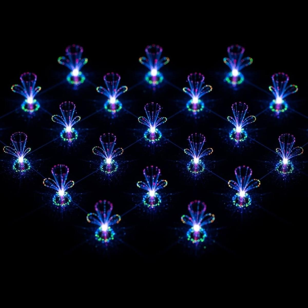
Superradiance, the collective acceleration of photon emission first described by Dicke, has long been confined to low‑temperature atoms or engineered cavities. Achieving the same effect in a solid‑state platform at ambient conditions removes a major barrier for scalable quantum technologies, promising faster, brighter sources that can be integrated on chips. Hexagonal boron nitride, a two‑dimensional wide‑bandgap material, offers atomically thin layers and naturally occurring point defects that act as quantum emitters, making it an ideal testbed for exploring cooperative optics without the need for bulky resonators.
In the reported study, researchers used focused electron‑beam irradiation to generate B‑center defect ensembles spaced within a sub‑wavelength volume. Confocal microscopy and Hanbury Brown‑Twiss interferometry identified clusters of one to four emitters, while time‑resolved photoluminescence revealed a monotonic shortening of radiative lifetimes as the emitter count increased, reaching the instrument’s 500 ps limit. Complementary g^(2)(0) measurements showed sub‑Poissonian antibunching, confirming that the enhanced emission stems from coherent coupling among a few indistinguishable defects rather than mere intensity scaling.
The ability to harness room‑temperature superradiance in hBN opens immediate pathways for commercial quantum devices. Ultrabright, fast‑decaying light sources can improve quantum key distribution rates, enable on‑chip quantum simulators, and simplify the design of quantum sensors that operate outside laboratory environments. Moreover, the cavity‑free nature of the platform reduces fabrication complexity and cost, encouraging integration with existing semiconductor manufacturing lines. Future work will likely focus on electrical injection, deterministic placement of defect ensembles, and scaling to larger photonic circuits, positioning hBN as a cornerstone material for the next generation of quantum photonic infrastructure.
Researchers Demonstrate Collective Emission from Hexagonal Boron Nitride Emitter Ensembles
0
Comments
Want to join the conversation?
Loading comments...