Researchers Unveil 1,400‑transistor MoS₂ Chip, a Milestone for 2D Computing
Why It Matters
The MoS₂ processor validates that transition‑metal dichalcogenides can be scaled to the transistor counts required for practical computing, challenging the notion that 2D materials are confined to laboratory curiosities. By delivering a functional 4‑bit processor with over 1,400 transistors, the work demonstrates a viable route to ultra‑low‑power chips for edge AI, where energy efficiency is paramount. Moreover, the MLCO design framework provides a reproducible methodology that other research groups and manufacturers can adopt, potentially accelerating the transition from silicon‑centric roadmaps to heterogeneous stacks that incorporate 2D layers for specialized functions. Beyond immediate technical relevance, the achievement could influence investment decisions in nanofabrication equipment, material supply chains for high‑purity MoS₂, and talent pipelines focused on 2D device engineering. As AI continues to drive demand for compute that can operate within tight power envelopes, the ability to replace or augment silicon with atomically thin semiconductors may become a strategic differentiator for companies seeking to stay ahead of the post‑Moore era. Finally, the collaboration between academia (Nanjing University), a national research hub (Suzhou Laboratory) and an industry leader (Huawei) illustrates a model for translating cutting‑edge nanotech research into manufacturable technology. This partnership could inspire similar consortia worldwide, fostering a more diversified semiconductor ecosystem that mitigates supply‑chain risks associated with reliance on a single material platform.
Key Takeaways
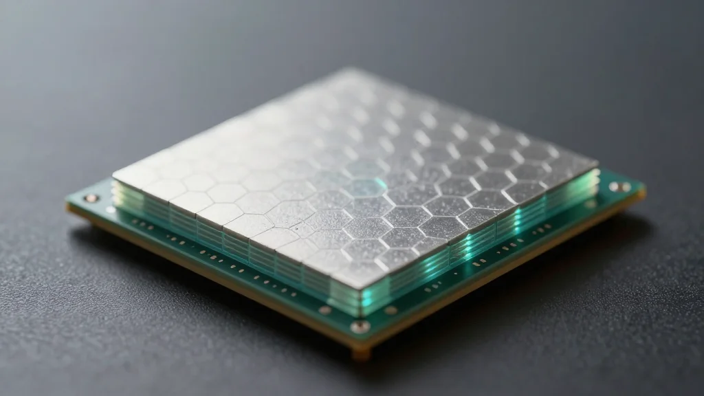
- •More than 1,400 MoS₂ transistors integrated on a single 4‑bit processor chip
- •MLCO methodology spans fabrication to logic synthesis, enabling end‑to‑end 2D chip design
- •Processor executes eight instructions across four core modules, a first for 2D‑material computers
- •Demonstrates potential for ultra‑low‑power AI edge devices where silicon faces scaling limits
- •Next steps include 8‑bit/16‑bit designs and real‑world AI inference demonstrations
Pulse Analysis
The MoS₂ processor represents a watershed moment for the nanotech sector, but its commercial impact will depend on how quickly the MLCO workflow can be industrialized. Historically, breakthroughs in material science—such as the transition from planar silicon to fin‑FETs—required a confluence of process engineering, design automation and ecosystem support. Here, the researchers have already addressed the design automation gap by publishing a complete flow, yet the manufacturing gap remains sizable. Wafer‑scale uniformity of MoS₂, defect control, and integration with existing CMOS back‑ends are non‑trivial challenges that could dictate the timeline for volume production.
From a market perspective, the chip arrives at a juncture where edge AI devices are proliferating across IoT, automotive and wearable segments. These markets prioritize power per operation over raw performance, a niche where 2D semiconductors excel. If the consortium can demonstrate a 2D processor that runs a neural network inference with sub‑millijoule energy consumption, it could attract early adopters willing to pay a premium for battery life extensions. However, incumbent silicon vendors are already pushing gate‑all‑around (GAA) and nanosheet technologies that promise similar power savings, meaning MoS₂ must carve out a differentiated value proposition—perhaps through flexibility, transparency or integration with photonic components.
Strategically, the involvement of Huawei signals a potential shift in the global semiconductor landscape. With access to extensive fabrication capacity and a vested interest in reducing reliance on foreign chip technologies, Huawei could accelerate the path from prototype to pilot production. This could spur other Chinese and international firms to invest in 2D material fabs, reshaping the competitive dynamics of the semiconductor supply chain. In the longer term, the success of MoS₂ processors may catalyze a broader move toward heterogeneous integration, where silicon handles high‑performance cores while 2D layers provide ultra‑low‑power accelerators, creating a new class of hybrid chips tailored for AI‑centric workloads.
Researchers unveil 1,400‑transistor MoS₂ chip, a milestone for 2D computing
Comments
Want to join the conversation?
Loading comments...