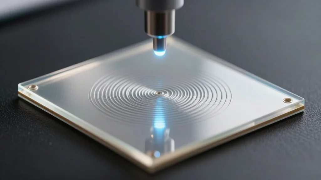
Rice University Demonstrates Room‑Temp Nanopatterning of Hard Chips with Stressed Crystal

Why It Matters
The ability to pattern hard, insulating materials at room temperature with a single electron‑beam step addresses a critical bottleneck in photonic chip production, where existing methods are either too costly or incompatible with standard semiconductor workflows. By reducing process complexity, the technique could accelerate the deployment of on‑chip optical interconnects, sensors, and quantum‑photonic components, all of which rely on precise nanoscale gratings. Moreover, the low‑temperature nature of the method aligns with the industry's push toward energy‑efficient manufacturing, potentially lowering the carbon footprint of future chip fabs. Beyond photonics, the approach may inspire new strategies for integrating nanostructures into a broader range of devices, from MEMS to flexible electronics, where patterning on rigid substrates has been a persistent challenge. If the method proves scalable, it could become a standard tool in the nanofabrication toolbox, reshaping how engineers think about material deformation and stress engineering at the nanoscale.
Key Takeaways
- •Rice University researchers use alpha‑molybdenum trioxide to create nanoscale ripples on silica at room temperature.
- •The electron‑beam process requires a single step and no high‑temperature or chemical treatments.
- •Patterns act as optical gratings, enabling light manipulation directly on hard chip materials.
- •Funding includes Army Research Office grant W911NF‑25‑1‑0265 and multiple NSF awards.
- •Next phase: pilot production in a commercial fab to test scalability and integration.
Pulse Analysis
The stressed‑crystal technique arrives at a moment when the semiconductor industry is scrambling to embed photonic functionality without inflating manufacturing costs. Historically, integrating optics has required dedicated process modules—such as silicon‑on‑insulator waveguide patterning—that add both capital expense and cycle time. By leveraging intrinsic crystal anisotropy, Rice's method sidesteps these extra modules, offering a plug‑and‑play solution that could be retrofitted onto existing fabs.
From a competitive standpoint, the approach pits itself against established nano‑imprint lithography (NIL) and electron‑beam direct write (EBDW) techniques. NIL delivers high throughput but demands a soft resist layer, while EBDW provides flexibility at the expense of speed and cost. The stressed‑crystal method blends the precision of EBDW with the material compatibility of NIL, potentially carving out a niche for low‑volume, high‑performance photonic devices where design agility outweighs sheer throughput.
Looking ahead, the key to commercial adoption will be the method's ability to maintain pattern fidelity across 300‑mm wafers and to survive subsequent high‑temperature steps such as dopant activation. If Rice can demonstrate that the peeled‑off crystal leaves no residue and that the wrinkles remain stable under thermal cycling, the industry may see a rapid uptake, especially among defense and communications firms eager for compact, integrated photonic solutions. The public funding backing suggests a strategic interest in maintaining U.S. leadership in next‑generation chip technologies, positioning this research as both a scientific breakthrough and a potential economic catalyst.
Rice University Demonstrates Room‑Temp Nanopatterning of Hard Chips with Stressed Crystal
Comments
Want to join the conversation?
Loading comments...