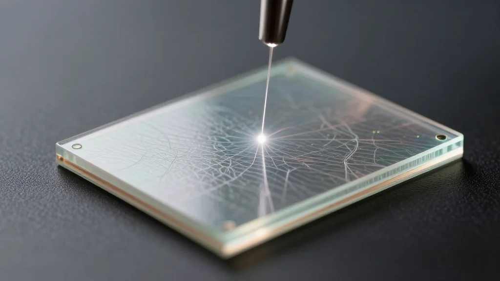
Room‑Temperature Electron Beam Technique Enables Nanoscale Chip Patterning

Why It Matters
The ability to pattern hard, insulating materials at room temperature removes a major hurdle for integrating photonic components directly onto electronic chips. Current photonic‑electronic co‑designs often require separate fabrication tracks, increasing complexity and cost. By providing a single‑step, low‑temperature route, the technique could enable tighter coupling of light‑based communication channels with conventional transistors, boosting data throughput while lowering power consumption. Beyond cost savings, the method’s reliance on electron‑beam tools—already present in many research and pilot fabs—means that scaling to production may be faster than for entirely new lithography platforms. If manufacturers adopt the approach, it could shorten the development cycle for emerging applications such as on‑chip lidar for autonomous vehicles, quantum information processors that need precise optical routing, and bio‑sensing arrays that combine electronic readout with optical interrogation.
Key Takeaways
- •Rice University scientists use an electron beam plus alpha‑molybdenum trioxide to pattern silica at room temperature.
- •The process creates nanoscale ripples only a few hundred nanometers wide in a single step.
- •Patterns act as optical gratings, enabling light manipulation on chip without high‑temperature steps.
- •Technique works on rigid insulating substrates, overcoming the need for soft, elastic layers.
- •Potential to lower cost and environmental impact of photonic‑electronic chip manufacturing.
Pulse Analysis
The breakthrough arrives at a pivotal moment when the semiconductor sector is pivoting from pure scaling to heterogeneous integration. Historically, adding photonic functionality has required dedicated foundry modules, often involving high‑temperature anneals that can damage existing electronic layers. By demonstrating a room‑temperature, electron‑beam‑driven stress method, the Rice team offers a bridge between the two worlds that could be adopted with minimal capital outlay.
From a competitive standpoint, incumbents such as Intel and TSMC have invested heavily in silicon‑photonic platforms, but their roadmaps still depend on complex multi‑step processes. A simpler, single‑step technique could erode the cost advantage of these giants, especially for niche players focused on high‑volume, low‑margin applications like data‑center interconnects. Moreover, the method’s reliance on electron‑beam equipment—already a staple in mask‑making and defect inspection—means that existing infrastructure can be repurposed, shortening the time to market.
Looking ahead, the key challenge will be translating laboratory‑scale exposures to wafer‑scale throughput. Electron‑beam lithography is traditionally slower than optical lithography, but recent advances in multi‑beam systems and parallel processing could mitigate this limitation. If the scalability hurdle is cleared, the technique could become a cornerstone of the next wave of photonic‑electronic convergence, enabling new architectures for AI accelerators, quantum processors, and ultra‑low‑power sensors.
Room‑Temperature Electron Beam Technique Enables Nanoscale Chip Patterning
Comments
Want to join the conversation?
Loading comments...