Russian Team Unveils Nanolaser with Record‑Narrow 0.15 Nm Emission Line
Why It Matters
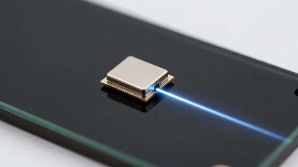
The nanolaser’s record‑narrow line width dramatically improves spectral purity, a critical parameter for high‑resolution sensing and low‑noise communication links. By shrinking the active region to 60 nm, the device can be embedded directly into photonic integrated circuits, reducing the need for bulky external lasers and enabling on‑chip light sources for next‑generation data centers and quantum devices. Moreover, the breakthrough demonstrates that Russian research institutions can achieve world‑class performance despite limited access to imported precision optics, potentially reshaping the competitive dynamics of the global nanophotonics market. In practical terms, the technology could accelerate the rollout of ultrasensitive biochemical detectors capable of identifying trace molecules in medical diagnostics or environmental monitoring. It also paves the way for super‑resolution microscopy tools that surpass current diffraction limits, benefitting both academic research and industrial quality control. The scalability of the nitride nanocrystal platform means that a single manufacturing line could serve multiple wavelength regimes, from UV sterilization lasers to infrared telecom components, consolidating supply chains and lowering costs. The broader strategic implication is a reduction in technological dependence for Russia’s defense and communications sectors. By internalizing a key component of photonic chips, the country can mitigate the impact of export controls and maintain a degree of autonomy in critical infrastructure.
Key Takeaways
- •Nanolaser emission line width measured at 0.15 nm, 5‑10× narrower than standard lasers
- •Active region size limited to 60 nm, enabling on‑chip integration
- •Developed by SPbSU, Alferov University, HSE, LETI, MIPT and foreign collaborators
- •Potential applications include biochemical sensors, super‑resolution microscopy, and photonic integrated circuits
- •Technology offers a sanctions‑resilient path for Russian optical chip production
Pulse Analysis
The Russian nanolaser marks a rare instance where geopolitical constraints have spurred a home‑grown innovation that rivals, and in some metrics exceeds, Western equivalents. Historically, breakthroughs in nanophotonics have been driven by large‑scale semiconductor fabs in the United States, Japan, and South Korea, where access to ultra‑pure substrates and advanced epitaxy tools is taken for granted. By leveraging molecular‑beam epitaxy on a metal‑dielectric substrate, the Russian team sidestepped the need for imported high‑precision optics, turning a limitation into a competitive advantage.
From a market perspective, the ability to produce sub‑100 nm lasers with ultra‑narrow line widths could disrupt the supply chain for photonic integrated circuits (PICs). Current PIC manufacturers rely on external laser sources that add cost, footprint, and alignment complexity. An on‑chip laser of this caliber could streamline designs, lower power consumption, and improve overall system stability—attributes that are especially valuable for data‑center interconnects and emerging quantum communication networks.
Looking ahead, the key challenge will be scaling the fabrication process. Molecular‑beam epitaxy is notoriously slow and expensive, and achieving uniform nanocrystal quality across wafer‑scale production will test the limits of existing Russian manufacturing infrastructure. If the team can demonstrate reproducible yields and integrate the lasers into commercial PIC platforms, they could capture a niche segment of the global market that values security‑by‑design and supply‑chain independence. Even if commercial uptake is modest, the scientific impact is undeniable: a 0.15 nm line width sets a new benchmark that will push competitors worldwide to refine their own nanolaser technologies.
Russian Team Unveils Nanolaser with Record‑Narrow 0.15 nm Emission Line
Comments
Want to join the conversation?
Loading comments...