Russian Team Unveils Nanolaser with Record‑Pure 0.15 Nm Linewidth
Why It Matters
The record‑narrow linewidth demonstrates that nanophotonic devices can achieve spectral purity previously thought attainable only with larger, more complex structures. This breakthrough could shrink the size and power budget of optical components in data centers, telecommunications, and biomedical instrumentation, accelerating the broader adoption of photonic integrated circuits. In the context of international sanctions, the development provides Russia with a domestically sourced, high‑performance light source, reducing reliance on imported precision optics. The technology’s scalability across UV to IR wavelengths also positions it as a versatile platform for future quantum‑communication links and on‑chip sensing solutions, potentially reshaping competitive dynamics in the global nanotech market.
Key Takeaways
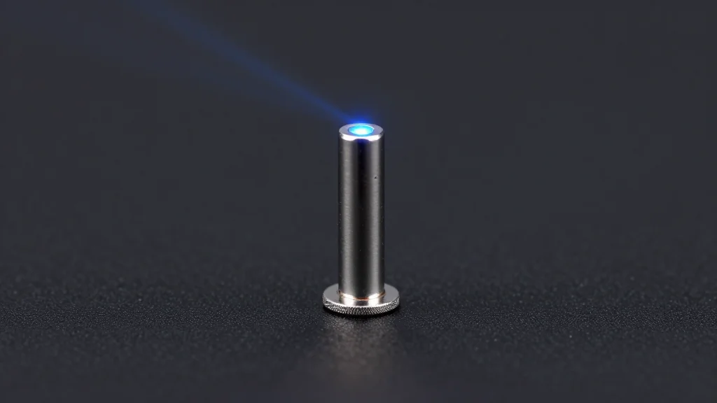
- •Emission linewidth measured at 0.15 nm, 5‑10× narrower than typical nanolasers
- •Active region size limited to ≤60 nm, the smallest reported to date
- •Design uses InGaN nanocrystals grown by molecular‑beam epitaxy on metal‑dielectric substrate
- •Collaboration spans SPbSU, Alferov University, HSE, LETI, MIPT and foreign researchers
- •Potential applications include biochemical sensors, super‑resolution microscopy, and photonic integrated circuits
Pulse Analysis
The 0.15 nm linewidth marks a decisive step forward in the quest for ultra‑compact, high‑coherence light sources. Historically, nanolasers have struggled with broad spectral output due to material imperfections and cavity losses; achieving a linewidth an order of magnitude tighter suggests that the Russian team has mastered surface‑smoothness and impurity control at a scale few labs can replicate.
From a market perspective, the ability to embed such a laser directly onto a photonic chip could disrupt the current supply chain dominated by larger III‑V semiconductor lasers and external cavity designs. Companies like Intel and IBM have invested heavily in heterogeneous integration to bring lasers onto silicon, but they still contend with size and thermal constraints. A sub‑60 nm laser could enable denser wavelength‑division multiplexing and lower energy per bit, giving early adopters a competitive edge in data‑center interconnects.
Geopolitically, the development showcases how sanctions can spur domestic innovation. By leveraging a nitride‑based platform that sidesteps restricted optical components, Russian researchers have created a self‑sufficient pathway to next‑generation photonics. However, scaling molecular‑beam epitaxy to high‑volume production will require substantial capital investment and may be hampered by limited access to advanced epitaxy equipment. If these hurdles are overcome, the technology could position Russia as a niche supplier of ultra‑compact lasers for specialized applications, while also prompting Western firms to accelerate their own linewidth‑reduction programs to maintain a performance lead.
Russian Team Unveils Nanolaser with Record‑Pure 0.15 nm Linewidth
Comments
Want to join the conversation?
Loading comments...