Samsung Breaks 10nm Barrier with First Single‑Digit Nanometer DRAM Die
Companies Mentioned
Why It Matters
Crossing the 10 nm threshold in DRAM production reshapes the competitive dynamics of the memory market. Samsung’s lead could translate into higher margins and stronger bargaining power with OEMs that require ever‑greater memory density. Moreover, the ability to produce functional sub‑10 nm dies validates the economic viability of next‑generation EUV lithography, encouraging further investment in the technology across the semiconductor ecosystem. For end‑users, the breakthrough promises faster, more power‑efficient devices. As AI workloads and cloud services continue to expand, the demand for memory that can store more data in a smaller footprint becomes critical. Samsung’s progress may accelerate the rollout of next‑generation servers and edge devices, influencing everything from data‑center economics to consumer gadget performance.
Key Takeaways
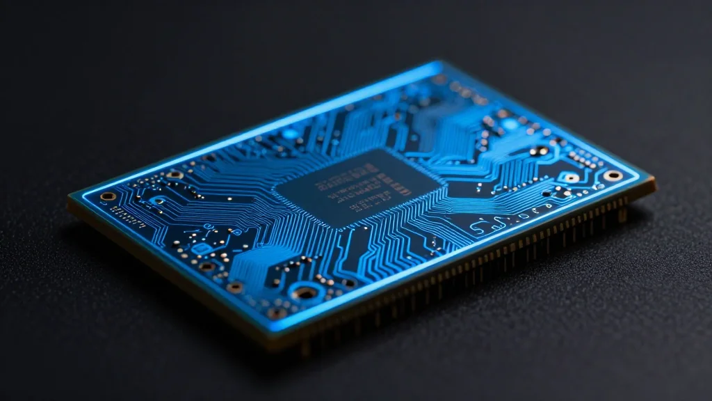
- •Samsung produced the world’s first single‑digit nanometer DRAM working die (10a DRAM).
- •The prototype is being used to refine process conditions and improve yield.
- •Industry analysts see the breakthrough as a potential 12‑18 month path to pilot production.
- •Success could boost demand for ASML’s EUV tools and advanced material suppliers.
- •Sub‑10 nm DRAM promises higher capacity per wafer and lower power consumption for AI and cloud workloads.
Pulse Analysis
Samsung’s sub‑10 nm DRAM milestone is more than a technical footnote; it is a strategic inflection point. Historically, each DRAM node shrink has delivered roughly a 20‑30% improvement in capacity‑per‑watt, and the move into single‑digit nanometers could double that gain. This advantage will be especially valuable as AI accelerators demand ever‑larger memory pools with tighter latency budgets.
From a market perspective, Samsung’s lead forces competitors to accelerate their own roadmaps. Micron and SK Hynix have publicly committed resources to sub‑10 nm research, but without a working die they risk falling behind in the next product cycle. The pressure may also spill over to foundries that supply logic chips, prompting a convergence of memory and compute scaling efforts. If Samsung can achieve high yields, it will likely command premium pricing for early‑adopter customers, reinforcing its position as the dominant DRAM supplier.
Looking forward, the real test will be volume production. Yield rates at sub‑10 nm are notoriously volatile, and any delay could erode the first‑mover advantage. However, Samsung’s integrated approach—combining in‑house design, advanced EUV lithography, and a deep supply chain—places it in a strong position to manage those risks. The next 12 months will reveal whether the 10a DRAM die remains a laboratory curiosity or becomes the foundation for the next generation of memory‑intensive systems.
Samsung Breaks 10nm Barrier with First Single‑Digit Nanometer DRAM Die
Comments
Want to join the conversation?
Loading comments...