Scaling Nanoribbon Transistors with Monolayer Transition Metal Dichalcogenides
Why It Matters
The work proves that atomically thin 2D semiconductors can scale below silicon’s 3 nm thickness limit, offering a realistic path to sub‑5 nm gate lengths and higher device density for next‑generation logic.
Key Takeaways
- •Anchored contacts give >85% yield for 60 nm nanoribbons
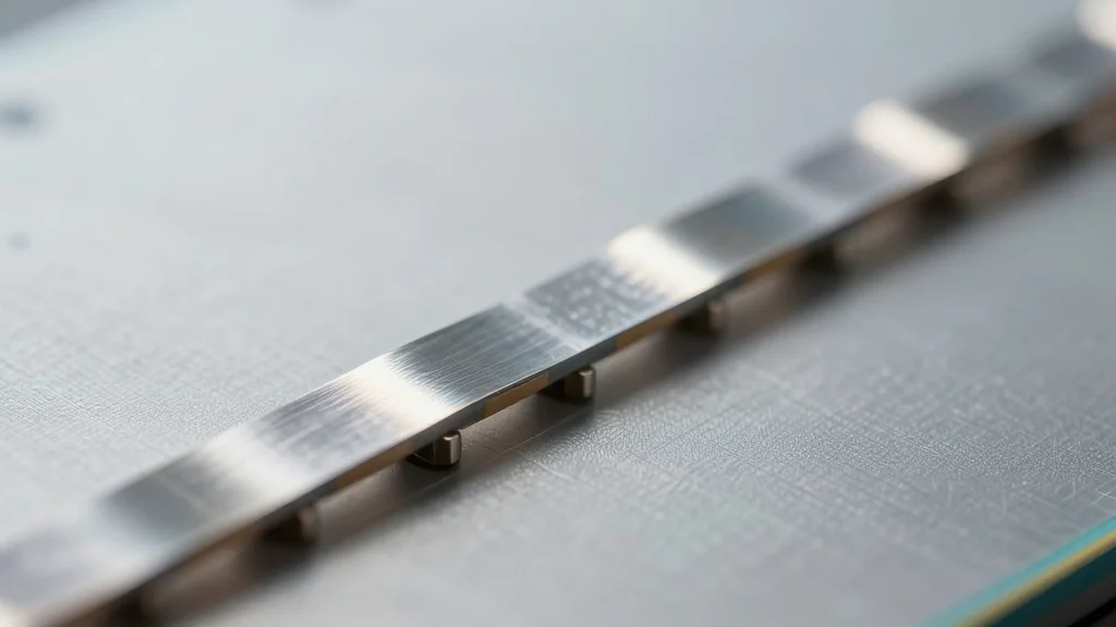
- •LELE multipatterning achieves 25 nm-wide monolayer TMD ribbons
- •MoS₂ nanoribbons deliver up to 620 µA µm⁻¹ current density
- •WS₂ ribbons show >100× current improvement, normally‑off behavior
- •Edge disorder does not limit performance down to 25 nm
Pulse Analysis
The semiconductor industry faces an imminent roadblock as silicon channels approach the physical limit of electrostatic control. While gate‑all‑around (GAA) nanosheets have extended Moore’s Law for another decade, further thickness reduction below 3 nm threatens mobility and reliability. Two‑dimensional materials, especially monolayer transition‑metal dichalcogenides, provide a compelling alternative because their sub‑nanometre thickness preserves carrier transport while enabling aggressive scaling of gate length and channel width. Integrating these 2D channels into a GAA architecture could unlock device densities previously unattainable with bulk silicon.
In the new study, the team tackled three critical challenges: mechanical stability, patterning precision, and contact resistance. By designing a dog‑bone‑shaped layout that anchors the nanoribbon under the contacts, they reduced delamination and achieved over 85% fabrication yield down to 60 nm. The LELE multipatterning process, borrowed from advanced CMOS manufacturing, pushed the minimum width to 25 nm without compromising the low‑dose exposure needed to avoid defect generation. Electrical measurements revealed current densities exceeding 600 µA µm⁻¹ for MoS₂ and a 100‑fold improvement for WS₂, with on/off ratios surpassing 10⁹, rivaling the best silicon GAA devices.
These results signal a tangible step toward incorporating 2D semiconductors into commercial logic. The demonstrated compatibility with high‑κ HfO₂ dielectrics and complementary n‑/p‑type operation aligns with existing CMOS process flows, reducing the integration barrier. As industry roadmaps project the need for sub‑5 nm gate lengths by the early 2030s, monolayer TMD nanoribbons could become the cornerstone of next‑generation low‑power, high‑performance processors, provided that large‑scale synthesis and uniformity challenges are addressed. Continued collaboration between academia and foundries will be essential to translate these laboratory breakthroughs into mass‑produced chips.
Scaling nanoribbon transistors with monolayer transition metal dichalcogenides
Comments
Want to join the conversation?
Loading comments...