Scientists Confirm One-Dimensional Electron Behavior in Phosphorus Chains
•February 16, 2026
0
Why It Matters
The ability to realize and verify true 1D electronic systems paves the way for novel quantum devices and could enable tunable semiconductor‑to‑metal transitions for nanoelectronics.
Key Takeaways
- •Phosphorus chains on silver show true 1D electron behavior.
- •ARPES isolated electronic signatures from three chain orientations.
- •DFT predicts semiconductor-to-metal transition with increased chain density.
- •Lateral interactions previously obscured 1D confinement now resolved.
- •Findings open path for 1D quantum material applications.
Pulse Analysis
Since the isolation of graphene, the materials community has chased ever‑thinner structures to unlock exotic electronic phenomena. Two‑dimensional crystals such as transition‑metal dichalcogenides have already demonstrated tunable band gaps, high carrier mobility, and strong spin‑orbit coupling. The logical next step—compressing electrons into a single spatial dimension—has remained largely theoretical because fabricating and probing true one‑dimensional (1D) systems is notoriously difficult. Phosphorus, a versatile element capable of forming both 2D layers and 1D chains, emerged as a promising candidate, but experimental confirmation of its 1D electronic character was missing—until now.
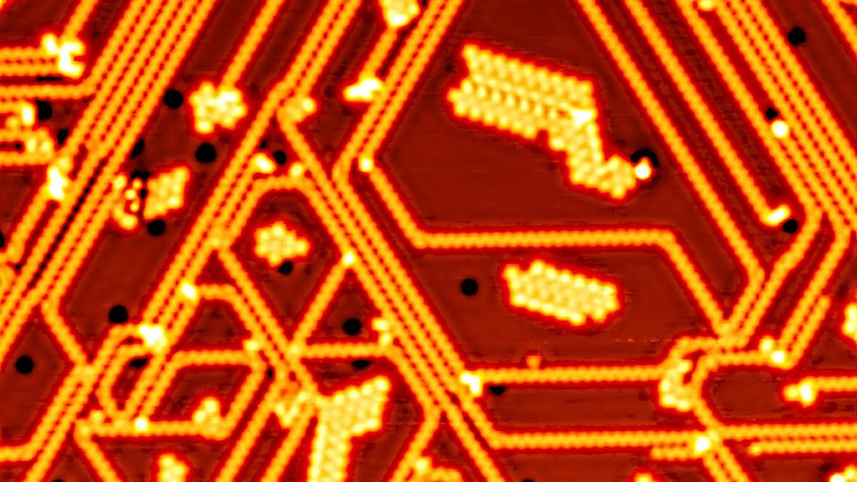
The BESSY II team combined cryogenic scanning tunnelling microscopy with high‑resolution angle‑resolved photoelectron spectroscopy to disentangle the overlapping signals from three crystallographically equivalent chain domains on a silver surface. By aligning the ARPES data with the STM‑identified orientations, they observed standing‑wave patterns and a linear dispersion that is characteristic of electrons confined to one dimension. Complementary density functional theory calculations reproduced the measured band structure and further predicted that reducing the inter‑chain spacing would collapse the semiconducting gap, driving a transition to metallic conductivity. This dual experimental‑theoretical approach eliminates the ambiguity that has plagued earlier studies.
The confirmation of a genuine 1D electronic system opens a new frontier for quantum device engineering. Materials that can switch between semiconducting and metallic states simply by adjusting chain density could serve as ultra‑compact switches, interconnects, or sensors in future nano‑architectures. Moreover, the pronounced electron‑electron interactions expected in 1D conductors may enable the exploration of Luttinger‑liquid behavior and topological excitations, enriching fundamental condensed‑matter research. As synthesis techniques improve, we can anticipate a broader class of atom‑scale wires, positioning phosphorus chains at the heart of next‑generation low‑dimensional electronics.
Scientists confirm one-dimensional electron behavior in phosphorus chains
0
Comments
Want to join the conversation?
Loading comments...